JAJSFU8D November 2017 – June 2024 ADS8166 , ADS8167 , ADS8168
PRODUCTION DATA
- 1
- 1 特長
- 2 アプリケーション
- 3 概要
- 4 Pin Configuration and Functions
- 5 Specifications
- 6 Detailed Description
-
7 Register Maps
- 7.1
Interface and Hardware Configuration Registers
- 7.1.1 REG_ACCESS Register (address = 00h) [reset = 00h]
- 7.1.2 PD_CNTL Register (address = 04h) [reset = 00h]
- 7.1.3 SDI_CNTL Register (address = 008h) [reset = 00h]
- 7.1.4 SDO_CNTL1 Register (address = 0Ch) [reset = 00h]
- 7.1.5 SDO_CNTL2 Register (address = 0Dh) [reset = 00h]
- 7.1.6 SDO_CNTL3 Register (address = 0Eh) [reset = 00h]
- 7.1.7 SDO_CNTL4 Register (address = 0Fh) [reset = 00h]
- 7.1.8 DATA_CNTL Register (address = 10h) [reset = 00h]
- 7.1.9 PARITY_CNTL Register (address = 11h) [reset = 00h]
- 7.2 Device Calibration Registers
- 7.3 Analog Input Configuration Registers
- 7.4
Channel Sequence Configuration Registers Map
- 7.4.1 DEVICE_CFG Register (address = 1Ch) [reset = 00h]
- 7.4.2 CHANNEL_ID Register (address = 1Dh) [reset = 00h]
- 7.4.3 SEQ_START Register (address = 1Eh) [reset = 00h]
- 7.4.4 SEQ_ABORT Register (address = 1Fh) [reset = 00h]
- 7.4.5 ON_THE_FLY_CFG Register (address = 2Ah) [reset = 00h]
- 7.4.6 AUTO_SEQ_CFG1 Register (address = 80h) [reset = 00h]
- 7.4.7 AUTO_SEQ_CFG2 Register (address = 82h) [reset = 00h]
- 7.4.8
Custom Channel Sequencing Mode Registers
- 7.4.8.1 CCS_START_INDEX Register (address = 88h) [reset = 00h]
- 7.4.8.2 CCS_END_INDEX Register (address = 89h) [reset = 00h]
- 7.4.8.3 CCS_SEQ_LOOP Register (address = 8Ah) [reset = 00h]
- 7.4.8.4 CCS_CHID_INDEX_m Registers (address = 8C, 8E, 90, 92, 94, 96, 98, 9A, 9C, 9E, A0, A2, A4, A6, A8, and AAh) [reset = 00h]
- 7.4.8.5 REPEAT_INDEX_m Registers (address = 8D, 8F, 91, 93, 95, 97, 99, 9B, 9D, 9F, A1, A3, A5, A7, A9, and ABh) [reset = 00h]
- 7.5
Digital Window Comparator Configuration Registers Map
- 7.5.1 ALERT_CFG Register (address = 2Eh) [reset = 00h]
- 7.5.2 HI_TRIG_AINx[15:0] Register (address = 4Dh to 30h) [reset = 0000h]
- 7.5.3 LO_TRIG_AINx[15:0] Register (address = 71h to 54h) [reset = 0000h]
- 7.5.4 HYSTERESIS_AINx[7:0] Register (address = 4Fh to 33h) [reset = 00h]
- 7.5.5 ALERT_LO_STATUS Register (address = 78h) [reset = 00h]
- 7.5.6 ALERT_HI_STATUS Register (address = 79h) [reset = 00h]
- 7.5.7 ALERT_STATUS Register (address = 7Ah) [reset = 00h]
- 7.5.8 CURR_ALERT_LO_STATUS Register (address = 7Ch) [reset = 00h]
- 7.5.9 CURR_ALERT_HI_STATUS Register (address = 7Dh) [reset = 00h]
- 7.5.10 CURR_ALERT_STATUS Register (address = 7Eh) [reset = 00h]
- 7.1
Interface and Hardware Configuration Registers
- 8 Application and Implementation
- 9 Device and Documentation Support
- 10Revision History
- 11Mechanical, Packaging, and Orderable Information
8.1.1 Multiplexer Input Connection
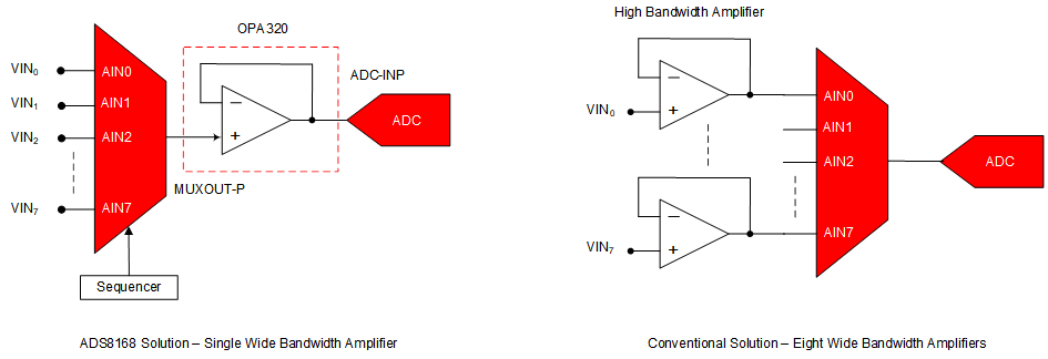
The ADS816x enables using a common amplifier to drive the ADC inputs as shown in Figure 8-1. This configuration improves offset error mismatch between the analog inputs as the offset error of the amplifier is common to all the analog input channels.
 Figure 8-1 Small-Size and Low-Power 8-Channel DAQ System Using the ADS816x
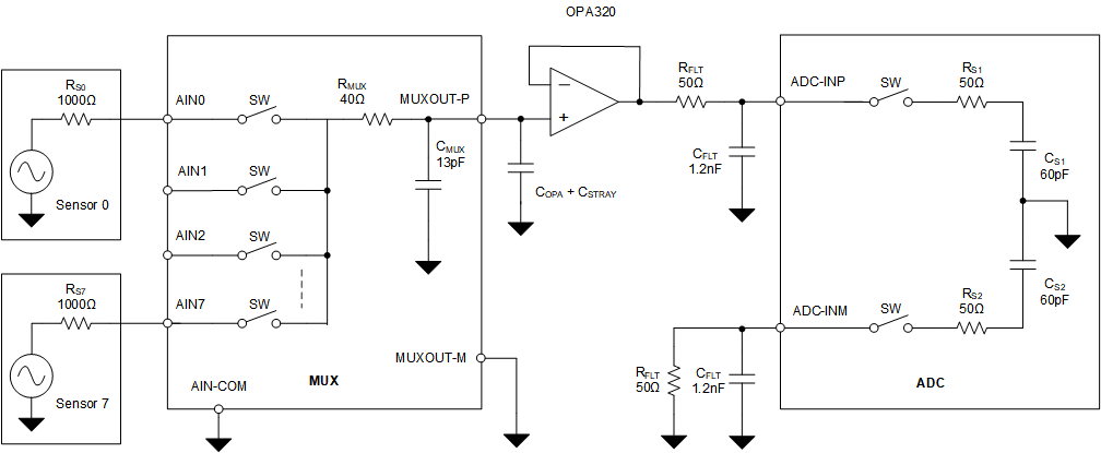
When connecting the sensor directly to the input of the ADS816x, the maximum switching speed of the multiplexer is limited by multiplexer on-resistance and parasitic capacitance. Figure 8-2 illustrates the source resistance (RS0, RS1, and so forth), multiplexer impedance (RMUX), multiplexer capacitance (CMUX), op amp input capacitance (COPA), and the stray PCB capacitance at the output of the multiplexer (CSTRAY). In this example, the total output capacitance is the combination of the multiplexer output capacitance, the op amp input capacitance, and the stray capacitance (CMUX + COPA + CSTRAY) = 15pF. When switching to a channel, make sure this capacitance is charged to the sensor output voltage with the source resistance and the multiplexer resistance (RS0 + RMUX).
Equation 2 estimates the number of time constants required for N bits of settling. For this example, to achieve 16-bit settling, 11.09 time constants are required. Thus, as computed in Equation 3 and Equation 4, for channel 0 the required settling time is 167ns.
 Figure 8-2 Direct Sensor Interface With the ADS816x in an 8-Channel, Single-Ended Configuration
When operating at 1MSPS in either manual mode, auto sequence mode, or custom channel sequencing mode, a 900ns settling time is available at the analog inputs of the multiplexer. Using Equation 4, the maximum sensor output impedance for a direct connection is 5.4kΩ.
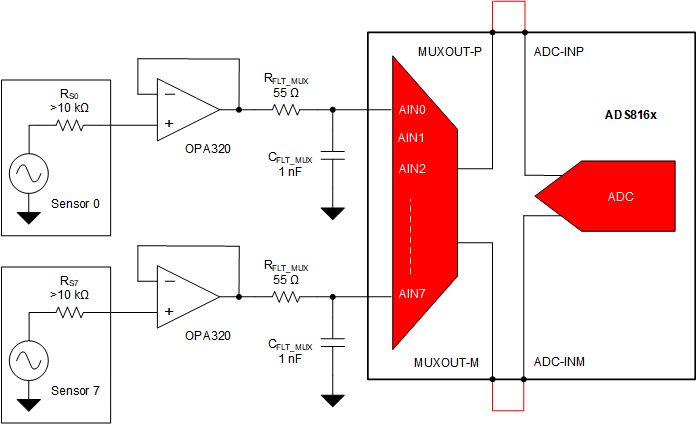
Figure 8-3 shows that the multiplexer inputs are driven using an amplifier. The multiplexer outputs are connected to the ADC inputs directly. For best distortion performance, place an amplifier between the multiplexer and the ADC as shown in Figure 8-2.
 Figure 8-3 High Output Impedance Sensor Interface