JAJSFY2B August 2018 – June 2021 LM5146-Q1
PRODUCTION DATA
- 1 特長
- 2 アプリケーション
- 3 概要
- 4 Revision History
- 5 概要 (続き)
- 6 Pin Configuration and Functions
- 7 Specifications
-
8 Detailed Description
- 8.1 Overview
- 8.2 Functional Block Diagram
- 8.3
Feature Description
- 8.3.1 Input Range (VIN)
- 8.3.2 Output Voltage Setpoint and Accuracy (FB)
- 8.3.3 High-Voltage Bias Supply Regulator (VCC)
- 8.3.4 Precision Enable (EN/UVLO)
- 8.3.5 Power Good Monitor (PGOOD)
- 8.3.6 Switching Frequency (RT, SYNCIN)
- 8.3.7 Configurable Soft Start (SS/TRK)
- 8.3.8 Voltage-Mode Control (COMP)
- 8.3.9 Gate Drivers (LO, HO)
- 8.3.10 Current Sensing and Overcurrent Protection (ILIM)
- 8.3.11 OCP Duty Cycle Limiter
- 8.4 Device Functional Modes
- 9 Application and Implementation
- 10Power Supply Recommendations
- 11Layout
- 12Device and Documentation Support
- 13Mechanical, Packaging, and Orderable Information
11.2 Layout Example
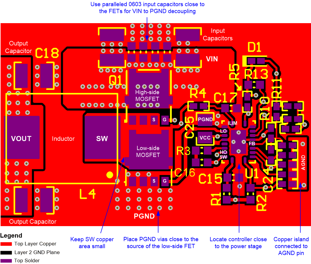
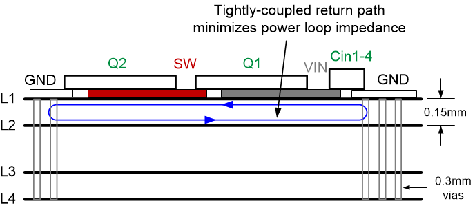
Figure 11-2 shows an example PCB layout based on the LM5146-Q1-EVM12V design. The power component connections are made on the top layer with wide, copper-filled polygon areas. The SW connection from the power MOSFETs to the inductor is purposely kept at minimum area to reduce radiated EMI. A power ground plane is placed on layer 2 with 6 mil (0.15 mm) spacing to the top layer, see Figure 11-3. As a result, the buck regulator hot loop has a small effective area based on this tightly-coupled GND plane directly underneath the MOSFETs.
The LM5146-Q1 controller is located close to the gate terminals of the MOSFETs such that the gate drive traces are routed short and direct. Refer to the LM5146-Q1-EVM12V Evaluation Module User's Guide for more detail.
 Figure 11-2 LM5146-Q1
Controller PCB Layout (Viewed From Top)