JAJSG17D June 2014 – August 2018 MSP430FR5986 , MSP430FR5987 , MSP430FR5988 , MSP430FR5989 , MSP430FR59891 , MSP430FR6987 , MSP430FR6988 , MSP430FR6989 , MSP430FR69891
PRODUCTION DATA.
- 1デバイスの概要
- 2改訂履歴
- 3Device Comparison
- 4Terminal Configuration and Functions
-
5Specifications
- 5.1 Absolute Maximum Ratings
- 5.2 ESD Ratings
- 5.3 Recommended Operating Conditions
- 5.4 Active Mode Supply Current Into VCC Excluding External Current
- 5.5 Typical Characteristics, Active Mode Supply Currents
- 5.6 Low-Power Mode (LPM0, LPM1) Supply Currents Into VCC Excluding External Current
- 5.7 Low-Power Mode (LPM2, LPM3, LPM4) Supply Currents (Into VCC) Excluding External Current
- 5.8 Low-Power Mode With LCD Supply Currents (Into VCC) Excluding External Current
- 5.9 Low-Power Mode LPMx.5 Supply Currents (Into VCC) Excluding External Current
- 5.10 Typical Characteristics, Low-Power Mode Supply Currents
- 5.11 Typical Characteristics, Current Consumption per Module
- 5.12 Thermal Resistance Characteristics
- 5.13
Timing and Switching Characteristics
- 5.13.1 Power Supply Sequencing
- 5.13.2 Reset Timing
- 5.13.3 Clock Specifications
- 5.13.4 Wake-up Characteristics
- 5.13.5
Peripherals
- 5.13.5.1 Digital I/Os
- 5.13.5.2 Timer_A and Timer_B
- 5.13.5.3 eUSCI
- 5.13.5.4 LCD Controller
- 5.13.5.5
ADC
- Table 5-24 12-Bit ADC, Power Supply and Input Range Conditions
- Table 5-25 12-Bit ADC, Timing Parameters
- Table 5-26 12-Bit ADC, Linearity Parameters With External Reference
- Table 5-27 12-Bit ADC, Dynamic Performance for Differential Inputs With External Reference
- Table 5-28 12-Bit ADC, Dynamic Performance for Differential Inputs With Internal Reference
- Table 5-29 12-Bit ADC, Dynamic Performance for Single-Ended Inputs With External Reference
- Table 5-30 12-Bit ADC, Dynamic Performance for Single-Ended Inputs With Internal Reference
- Table 5-31 12-Bit ADC, Dynamic Performance With 32.768-kHz Clock
- Table 5-32 12-Bit ADC, Temperature Sensor and Built-In V1/2
- Table 5-33 12-Bit ADC, External Reference
- 5.13.5.6 Reference
- 5.13.5.7 Comparator
- 5.13.5.8
Scan Interface
- Table 5-36 Extended Scan Interface, Port Drive, Port Timing
- Table 5-37 Extended Scan Interface, Sample Capacitor/Ri Timing
- Table 5-38 Extended Scan Interface, VCC/2 Generator
- Table 5-39 Extended Scan Interface, 12-Bit DAC
- Table 5-40 Extended Scan Interface, Comparator
- Table 5-41 Extended Scan Interface, ESICLK Oscillator and TSM Clock Signals
- 5.13.5.9 FRAM Controller
- 5.13.6 Emulation and Debug
-
6Detailed Description
- 6.1 Overview
- 6.2 CPU
- 6.3 Operating Modes
- 6.4 Interrupt Vector Table and Signatures
- 6.5 Bootloader (BSL)
- 6.6 JTAG Operation
- 6.7 FRAM
- 6.8 RAM
- 6.9 Tiny RAM
- 6.10 Memory Protection Unit Including IP Encapsulation
- 6.11
Peripherals
- 6.11.1 Digital I/O
- 6.11.2 Oscillator and Clock System (CS)
- 6.11.3 Power-Management Module (PMM)
- 6.11.4 Hardware Multiplier (MPY)
- 6.11.5 Real-Time Clock (RTC_C)
- 6.11.6 Watchdog Timer (WDT_A)
- 6.11.7 System Module (SYS)
- 6.11.8 DMA Controller
- 6.11.9 Enhanced Universal Serial Communication Interface (eUSCI)
- 6.11.10 Extended Scan Interface (ESI)
- 6.11.11 Timer_A TA0, Timer_A TA1
- 6.11.12 Timer_A TA2
- 6.11.13 Timer_A TA3
- 6.11.14 Timer_B TB0
- 6.11.15 ADC12_B
- 6.11.16 Comparator_E
- 6.11.17 CRC16
- 6.11.18 CRC32
- 6.11.19 AES256 Accelerator
- 6.11.20 True Random Seed
- 6.11.21 Shared Reference (REF_A)
- 6.11.22 LCD_C
- 6.11.23 Embedded Emulation
- 6.11.24
Input/Output Diagrams
- 6.11.24.1 Digital I/O Functionality – Ports P1 to P10
- 6.11.24.2 Capacitive Touch Functionality Ports P1 to P10 and PJ
- 6.11.24.3 Port P1 (P1.0 to P1.3) Input/Output With Schmitt Trigger
- 6.11.24.4 Port P1 (P1.4 to P1.7) Input/Output With Schmitt Trigger
- 6.11.24.5 Port P2 (P2.0 to P2.3) Input/Output With Schmitt Trigger
- 6.11.24.6 Port P2 (P2.4 to P2.7) Input/Output With Schmitt Trigger
- 6.11.24.7 Port P3 (P3.0 to P3.7) Input/Output With Schmitt Trigger
- 6.11.24.8 Port P4 (P4.0 to P4.7) Input/Output With Schmitt Trigger
- 6.11.24.9 Port P5 (P5.0 to P5.7) Input/Output With Schmitt Trigger
- 6.11.24.10 Port P6 (P6.0 to P6.6) Input/Output With Schmitt Trigger
- 6.11.24.11 Port P6 (P6.7) Input/Output With Schmitt Trigger
- 6.11.24.12 Port P7 (P7.0 to P7.7) Input/Output With Schmitt Trigger
- 6.11.24.13 Port P8 (P8.0 to P8.3) Input/Output With Schmitt Trigger
- 6.11.24.14 Port P8 (P8.4 to P8.7) Input/Output With Schmitt Trigger
- 6.11.24.15 Port P9 (P9.0 to P9.3) Input/Output With Schmitt Trigger
- 6.11.24.16 Port P9 (P9.4 to P9.7) Input/Output With Schmitt Trigger
- 6.11.24.17 Port P10 (P10.0 to P10.2) Input/Output With Schmitt Trigger
- 6.11.24.18 Port PJ (PJ.4 and PJ.5) Input/Output With Schmitt Trigger
- 6.11.24.19 Port PJ (PJ.6 and PJ.7) Input/Output With Schmitt Trigger
- 6.11.24.20 Port PJ (PJ.0 to PJ.3) JTAG Pins TDO, TMS, TCK, TDI/TCLK, Input/Output With Schmitt Trigger
- 6.12 Device Descriptors (TLV)
- 6.13 Memory
- 6.14 Identification
- 7Applications, Implementation, and Layout
- 8デバイスおよびドキュメントのサポート
- 9メカニカル、パッケージ、および注文情報
Table 5-20 eUSCI (SPI Slave Mode)
over recommended ranges of supply voltage and operating free-air temperature (unless otherwise noted)(1)| PARAMETER | TEST CONDITIONS | VCC | MIN | MAX | UNIT | |
|---|---|---|---|---|---|---|
| tSTE,LEAD | STE lead time, STE active to clock | 2.2 V | 45 | ns | ||
| 3.0 V | 40 | |||||
| tSTE,LAG | STE lag time, Last clock to STE inactive | 2.2 V | 2 | ns | ||
| 3.0 V | 3 | |||||
| tSTE,ACC | STE access time, STE active to SOMI data out | 2.2 V | 45 | ns | ||
| 3.0 V | 40 | |||||
| tSTE,DIS | STE disable time, STE inactive to SOMI high impedance | 2.2 V | 50 | ns | ||
| 3.0 V | 45 | |||||
| tSU,SI | SIMO input data setup time | 2.2 V | 4 | ns | ||
| 3.0 V | 4 | |||||
| tHD,SI | SIMO input data hold time | 2.2 V | 7 | ns | ||
| 3.0 V | 7 | |||||
| tVALID,SO | SOMI output data valid time(2) | UCLK edge to SOMI valid,
CL = 20 pF |
2.2 V | 35 | ns | |
| 3.0 V | 35 | |||||
| tHD,SO | SOMI output data hold time(3) | CL = 20 pF | 2.2 V | 0 | ns | |
| 3.0 V | 0 | |||||
(1) fUCxCLK = 1/2tLO/HI with tLO/HI ≥ max(tVALID,MO(Master) + tSU,SI(eUSCI), tSU,MI(Master) + tVALID,SO(eUSCI))
For the master parameters tSU,MI(Master) and tVALID,MO(Master), see the SPI parameters of the attached master.
For the master parameters tSU,MI(Master) and tVALID,MO(Master), see the SPI parameters of the attached master.
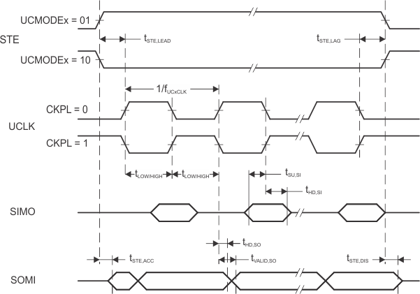
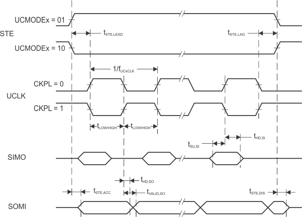
(2) Specifies the time to drive the next valid data to the SOMI output after the output changing UCLK clock edge. See the timing diagrams in Figure 5-17 and Figure 5-18.
(3) Specifies how long data on the SOMI output is valid after the output changing UCLK clock edge. See the timing diagrams inFigure 5-17 and Figure 5-18.
 Figure 5-17 SPI Slave Mode, CKPH = 0
  Figure 5-18 SPI Slave Mode, CKPH = 1
 Table 5-21 lists the characteristics of the eUSCI in I2C mode.