-
TCAN1044-Q1 車載用、フォルト保護機能搭載、1.8V I/O 対応、CAN FD トランシーバ
- 1
- 1 特長
- 2 アプリケーション
- 3 概要
- 4 Pin Configuration and Functions
- 5 Specifications
- 6 Parameter Measurement Information
-
7 Detailed Description
- 7.1 Overview
- 7.2 Functional Block Diagram
- 7.3 Feature Description
- 7.4 Device Functional Modes
- 8 Application and Implementation
- 9 Device and Documentation Support
- 10Revision History
- 11Mechanical, Packaging, and Orderable Information
- 重要なお知らせ
TCAN1044-Q1 車載用、フォルト保護機能搭載、1.8V I/O 対応、CAN FD トランシーバ
このリソースの元の言語は英語です。 翻訳は概要を便宜的に提供するもので、自動化ツール (機械翻訳) を使用していることがあり、TI では翻訳の正確性および妥当性につきましては一切保証いたしません。 実際の設計などの前には、ti.com で必ず最新の英語版をご参照くださいますようお願いいたします。
1 特長
- AEC-Q100:車載アプリケーション認定済み
- 温度グレード 1:–40℃~125℃ TA
- ISO 11898-2:2016 および ISO 11898-5:2007 物理層規格の要件に適合
- 機能安全対応
- Classical CAN のサポートと最適化された CAN FD 性能 (2、5、8Mbps)
- 短く対称的な伝搬遅延時間によりタイミング マージンを強化
- 負荷のある CAN ネットワークでより高いデータ レートを実現
- I/O 電圧範囲:1.7 V~5.5 V
- 1.8V、2.5V、3.3V、5V アプリケーションをサポート
- 保護機能:
- バス フォルト保護:±58 V
- 低電圧保護
- TXD ドミナント タイムアウト (DTO)
- 最小 9.2kbps のデータ レート
- サーマル シャットダウン保護 (TSD)
- 動作モード:
- 通常モード
- リモート ウェイクアップ要求をサポートする、低消費電力スタンバイ モード
- 電源非接続時の最適化された挙動
- バスおよびロジック ピンは高インピーダンス (動作中のバス、アプリケーションに対して無負荷)
- ホットプラグ対応:バスおよび RXD 出力での電源オン/オフ時のグリッチ フリー動作
- 接合部温度範囲:-40℃~150℃
- レシーバの同相入力電圧:±12 V
- SOIC (8)、SOT23 (8) パッケージ、
自動光学検査 (AOI) 性能を向上させたリードレス VSON (8) パッケージで供給
2 アプリケーション
- 車両および輸送システム
3 概要
TCAN1044-Q1 は、ISO 11898-2:2016 高速 CAN (Controller Area Network) 仕様の物理層要件を満たす高速 CAN トランシーバです。
TCAN1044-Q1 トランシーバは Classical CAN ネットワークおよび最高 8 メガビット/秒 (Mbps) の CAN FD ネットワークの両方に対応しています。TCAN1044-Q1 は VIO 端子によるロジック レベル変換機能を内蔵しているため、トランシーバの I/O を 1.8V、2.5V、3.3V、5V のロジック I/O に直接接続できます。このトランシーバは低消費電力スタンバイ モードと、ISO 11898-2:2016 に定義されたウェイクアップ パターン (WUP) に準拠した「CAN によるウェイク」をサポートしています。TCAN1044-Q1 トランシーバは、サーマル シャットダウン (TSD)、TXD ドミナント タイムアウト (DTO)、電源低電圧検出、最高 ±58V のバス フォルト保護に対応する保護および診断機能も備えています。
| 部品番号 | パッケージ (1) | パッケージ サイズ(2) |
|---|---|---|
| TCAN1044-Q1 | SOT (DDF、8) | 2.9 mm × 2.8mm |
| VSON (DRB、8) | 3 mm × 3mm | |
| SOIC (D、8) | 4.9 mm × 6mm |
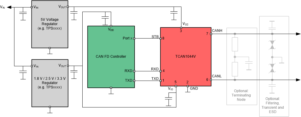 概略回路図
概略回路図4 Pin Configuration and Functions
(Top View)
(Top View)
(Top View)
| Pins | Type | Description | |
|---|---|---|---|
| Name | No. | ||
| TXD | 1 | Digital Input | CAN transmit data input |
| GND | 2 | GND | Ground connection |
| VCC | 3 | Supply | 5V supply voltage |
| RXD | 4 | Digital Output | CAN receive data output, tri-state when powered off |
| NC | 5 | — | No Connect (not internally connected); Devices without VIO |
| VIO | Supply | I/O supply voltage | |
| CANL | 6 | Bus IO | Low-level CAN bus input/output line |
| CANH | 7 | Bus IO | High-level CAN bus input/output line |
| STB | 8 | Digital Input | Standby input for mode control, integrated pull up |
| Thermal Pad (VSON only) | — | Electrically connected to GND, connect the thermal pad to the printed circuit board (PCB) ground plane for thermal relief | |
5 Specifications
5.1 Absolute Maximum Ratings
| MIN | MAX | UNIT | ||
|---|---|---|---|---|
| VCC | Supply voltage | –0.3 | 6 | V |
| VIO | Supply voltage I/O level shifter | –0.3 | 6 | V |
| VBUS | CAN Bus IO voltage CANH and CANL | –58 | 58 | V |
| VDIFF | Max differential voltage between CANH and CANL | –45 | 45 | V |
| VLogic_Input | Logic input terminal voltage | –0.3 | 6 | V |
| VRXD | RXD output terminal voltage range | –0.3 | 6 | V |
| IO(RXD) | RXD output current | –8 | 8 | mA |
| TJ | Operating virtual junction temperature range | –40 | 150 | °C |
| TSTG | Storage temperature | –65 | 150 | °C |
5.2 ESD Ratings
| VALUE | UNIT | ||||
|---|---|---|---|---|---|
| VESD | Electrostatic discharge | Human-body model (HBM), per AEC Q100-002(1) | HBM classification level 3A for all pins | ±3000 | V |
| HBM classification level 3B for global pins CANH & CANL | ±10000 | V | |||
| Charged-device model (CDM), per AEC Q100-011 CDM classification level C5 for all pins | ±750 | V | |||
5.3 ESD Ratings
| VALUE | UNIT | ||||
|---|---|---|---|---|---|
| VESD | System Level Electro-Static Discharge (ESD)(3) | CAN bus terminals (CANH, CANL) to GND | SAE J2962-2 per ISO 10650 Powered Contact Discharge |
±8000 | V |
| SAE J2962-2 per ISO 10650 Powered Air Discharge | ±15000 | V | |||
| VTran | ISO 7637 ISO Pulse Transients(1) | CAN bus terminals (CANH, CANL) | Pulse 1 | –100 | V |
| Pulse 2a | 75 | V | |||
| Pulse 3a | –150 | V | |||
| Pulse 3b | 100 | V | |||
| ISO 7637 Slow transients pulse(2) | CAN bus terminals (CANH, CANL) to GND | DCC slow transient pulse | ±85 | V | |
5.4 Recommended Operating Conditions
| MIN | NOM | MAX | UNIT | ||
|---|---|---|---|---|---|
| VCC | Supply voltage | 4.5 | 5 | 5.5 | V |
| VIO | Supply voltage for I/O level shifter | 1.7 | 5.5 | V | |
| IOH(RXD) | RXD terminal high level output current | –2 | mA | ||
| IOL(RXD) | RXD terminal low level output current | 2 | mA | ||
| TA | Operating ambient temperature | –40 | 125 | ℃ | |
5.5 Thermal Characteristics
| THERMAL METRIC(1) | TCAN1044x-Q1 | UNIT | |||
|---|---|---|---|---|---|
| D (SOIC) | DDF (SOT) | DRB (VSON) | |||
| RΘJA | Junction-to-ambient thermal resistance | 128.1 | 119.9 | 49.9 | ℃/W |
| RΘJC(top) | Junction-to-case (top) thermal resistance | 68.3 | 61.8 | 58.2 | ℃/W |
| RΘJB | Junction-to-board thermal resistance | 71.6 | 39.7 | 23.9 | ℃/W |
| ΨJT | Junction-to-top characterization parameter | 19.7 | 2.1 | 1.7 | ℃/W |
| ΨJB | Junction-to-board characterization parameter | 70.8 | 39.5 | 23.8 | ℃/W |
| RΘJC(bot) | Junction-to-case (bottom) thermal resistance | - | – | 6.4 | ℃/W |
5.6 Supply Characteristics
| PARAMETER | TEST CONDITIONS | MIN | TYP | MAX | UNIT | ||
|---|---|---|---|---|---|---|---|
| ICC | Supply current Normal mode | Dominant | TXD = 0 V, STB = 0 V, RL = 60 Ω, CL = open See Figure 6-1 | 45 | 70 | mA | |
| TXD = 0 V, STB = 0 V, RL = 50 Ω, CL = open See Figure 6-1 | 49 | 80 | mA | ||||
| Recessive | TXD = VCC, STB = 0 V, RL = 50 Ω, CL = open See Figure 6-1 | 4.5 | 7.5 | mA | |||
| Dominant with bus fault | TXD = 0 V, STB = 0 V, CANH = CANL = ±25 V, RL = open, CL = open See Figure 6-1 | 130 | mA | ||||
| ICC | Supply current Standby mode Devices with VIO | TXD = STB = VIO, RL = 50 Ω, CL = open See Figure 6-1 | 0.2 | 1 | µA | ||
| ICC | Supply current Standby mode Devices without VIO | TXD = STB = VCC, RL = 50 Ω, CL = open See Figure 6-1 | 14.5 | µA | |||
| IIO | I/O supply current Normal mode | Dominant | TXD = 0 V, STB= 0 V RXD floating | 125 | 300 | µA | |
| IIO | I/O supply current Normal mode | Recessive | TXD = 0 V, STB = 0 V RXD floating | 25 | 48 | µA | |
| IIO | I/O supply current Standby mode | TXD = 0 V, STB = VIO RXD floating | 8.5 | 13.5 | µA | ||
| UVVCC | Rising under voltage detection on VCC for protected mode | 4.2 | 4.4 | V | |||
| UVVCC | Falling under voltage detection on VCC for protected mode | 3.5 | 4 | 4.25 | V | ||
| UVVIO | Rising under voltage detection on VIO (Devices with VIO) | 1.56 | 1.65 | V | |||
| UVVIO | Falling under voltage detection on VIO (Devices with VIO) | 1.4 | 1.51 | 1.59 | V | ||
5.7 Dissipation Ratings
| PARAMETER | TEST CONDITIONS | MIN | TYP | MAX | UNIT | |
|---|---|---|---|---|---|---|
| PD | Average power dissipation Normal mode | VCC = 5 V, VIO = 1.8 V, TJ= 27°C, RL = 60Ω, TXD input = 250 kHz 50% duty cycle square wave, CL_RXD = 15 pF | 110 | mW | ||
| VCC = 5 V, VIO = 3.3 V, TJ= 27°C, RL = 60Ω, TXD input = 250 kHz 50% duty cycle square wave, CL_RXD = 15 pF | 110 | mW | ||||
| VCC = 5 V, VIO = 5 V, TJ= 27°C, RL = 60Ω, TXD input = 250 kHz 50% duty cycle square wave, CL_RXD = 15 pF | 110 | mW | ||||
| VCC = 5.5 V, VIO = 1.8 V, TA= 125°C, RL = 60Ω, TXD input = 2.5 MHz 50% duty cycle square wave, CL_RXD = 15 pF | 120 | mW | ||||
| VCC = 5.5 V, VIO = 3.3 V, TA= 125°C, RL = 60Ω, TXD input = 2.5 MHz 50% duty cycle square wave, CL_RXD = 15 pF | 120 | mW | ||||
| VCC = 5.5 V, VIO = 5 V, TA= 125°C, RL = 60Ω, TXD input = 2.5 MHz 50% duty cycle square wave, CL_RXD = 15 pF | 120 | mW | ||||
| TTSD | Thermal shutdown temperature | 192 | °C | |||
| TTSD_HYS | Thermal shutdown hysteresis | 10 | ||||
5.8 Electrical Characteristics
| PARAMETER | TEST CONDITIONS | MIN | TYP | MAX | UNIT | ||
|---|---|---|---|---|---|---|---|
| Driver Electrical Characteristics | |||||||
| VO(DOM) | Dominant output voltage Normal mode | CANH | TXD = 0 V, STB = 0 V, 50 Ω ≤ RL ≤ 65 Ω, CL =
open, RCM = open See Figure 6-2 and Figure 7-3, |
2.75 | 4.5 | V | |
| CANL | 0.5 | 2.25 | V | ||||
| VO(REC) | Recessive output voltage Normal mode | CANH and CANL | TXD = VIO, STB = 0 V, RL = open (no load),
RCM = open See Figure 6-2 and Figure 7-3 |
2 | 0.5 VCC | 3 | V |
| VSYM | Driver symmetry (VO(CANH) + VO(CANL))/VCC |
STB = 0 V, RL = 60 Ω, CSPLIT = 4.7
nF, CL = open, RCM = open, TXD = 250 kHz, 1
MHz, 2.5 MHz See Figure 6-2 and Figure 8-2 |
0.9 | 1.1 | V/V | ||
| VSYM_DC | DC output symmetry (VCC - VO(CANH) - VO(CANL)) |
STB = 0 V, RL = 60 Ω, CL = open See Figure 6-2 and Figure 7-3 |
–400 | 400 | mV | ||
| VOD(DOM) | Differential output voltage Normal mode Dominant |
CANH - CANL | TXD = 0 V, STB = 0 V, 50 Ω ≤ RL ≤ 65 Ω, CL =
open See Figure 6-2 and Figure 7-3 |
1.5 | 3 | V | |
| TXD = 0 V, STB = 0 V, 45 Ω ≤ RL ≤ 70 Ω, CL =
open See Figure 6-2 and Figure 7-3 |
1.4 | 3.3 | V | ||||
| TXD = 0 V, STB = 0 V, RL = 2240 Ω, CL = open See Figure 6-2 and Figure 7-3 |
1.5 | 5 | V | ||||
| VOD(REC) | Differential output voltage Normal mode Recessive |
CANH - CANL | TXD = VIO, STB = 0 V, RL = 60 Ω, CL = open See Figure 6-2 and Figure 7-3 |
–120 | 12 | mV | |
| TXD = VIO, STB = 0 V, RL = open, CL = open See Figure 6-2 and Figure 7-3 |
–50 | 50 | mV | ||||
| VO(STB) | Bus output voltage Standby mode |
CANH | STB = VIO, RL = open (no load) See Figure 6-2 and Figure 7-3 |
-0.1 | 0.1 | V | |
| CANL | -0.1 | 0.1 | V | ||||
| CANH - CANL | -0.2 | 0.2 | V | ||||
| IOS(SS_DOM) | Short-circuit steady-state output
current, dominant Normal mode |
STB = 0 V, V(CANH) = -15 V to 40 V, CANL =
open, TXD = 0 V See Figure 6-7 and Figure 7-3 |
–115 | mA | |||
| STB = 0 V, V(CAN_L) = -15 V to 40 V, CANH =
open, TXD = 0 V See Figure 6-7 and Figure 7-3 |
115 | mA | |||||
| IOS(SS_REC) | Short-circuit steady-state output current,
recessive Normal mode |
STB = 0 V, –27 V ≤ VBUS ≤ 32 V, where
VBUS = CANH = CANL, TXD = VIO See Figure 6-7 and Figure 7-3 |
–5 | 5 | mA | ||
| Receiver Electrical Characteristics | |||||||
| VIT | Input threshold voltage Normal mode |
STB = 0 V, -12 V ≤ VCM ≤ 12 V See Figure 6-3, Table 6-1, and Table 7-6 |
500 | 900 | mV | ||
| VIT(STB) | Input threshold Standby mode |
STB = VIO, -12 V ≤ VCM ≤ 12 V See Figure 6-3, Table 6-1, and Table 7-6 |
400 | 1150 | mV | ||
| VDOM | Dominant state differential input voltage range Normal mode |
STB = 0 V, -12 V ≤ VCM ≤ 12 V See Figure 6-3, Table 6-1, and Table 7-6 |
0.9 | 9 | V | ||
| VREC | Recessive state differential input voltage range Normal mode |
STB = 0 V, -12 V ≤ VCM ≤ 12 V See Figure 6-3, Table 6-1, and Table 7-6 |
-4 | 0.5 | V | ||
| VDOM(STB) | Dominant state differential input voltage range Standby mode |
STB = VIO, -12 V ≤ VCM ≤ 12 V See Figure 6-3, Table 6-1, and Table 7-6 |
1.15 | 9 | V | ||
| VREC(STB) | Recessive state differential input voltage range Standby mode |
STB = VIO, -12 V ≤ VCM ≤ 12 V See Figure 6-3, Table 6-1, and Table 7-6 |
-4 | 0.4 | V | ||
| VHYS | Hysteresis voltage for input threshold Normal mode |
STB = 0 V, -12 V ≤ VCM ≤ 12 V See Figure 6-3, Table 6-1, and Table 7-6 |
100 | mV | |||
| VCM | Common mode range Normal and standby modes |
See Figure 6-3 and Table 7-6Table 7-6 | –12 | 12 | V | ||
| ILKG(IOFF) | Unpowered bus input leakage current | CANH = CANL = 5 V, VCC = VIO = GND | 5 | µA | |||
| CI | Input capacitance to ground (CANH or CANL) | TXD = VIO(1) |
20 | pF | |||
| CID | Differential input capacitance | 10 | pF | ||||
| RID | Differential input resistance | TXD = VIO(1), STB = 0 V, -12 V ≤ VCM ≤ 12 V | 40 | 90 | kΩ | ||
| RIN | Single ended input resistance (CANH or CANL) |
20 | 45 | kΩ | |||
| RIN(M) | Input resistance matching [1 – (RIN(CANH) / RIN(CANL))] × 100 % |
V(CAN_H) = V(CAN_L) = 5 V | –1% | 1% | |||
| TXD Terminal (CAN Transmit Data Input) | |||||||
| VIH | High-level input voltage | Devices without VIO | 0.7 VCC | V | |||
| VIH | High-level input voltage | Devices with VIO | 0.7 VIO | V | |||
| VIL | Low-level input voltage | Devices without VIO | 0.3 VCC | V | |||
| VIL | Low-level input voltage | Devices with VIO | 0.3 VIO | V | |||
| IIH | High-level input leakage current | TXD = VCC = VIO = 5.5 V | –2.5 | 0 | 1 | µA | |
| IIL | Low-level input leakage current | TXD = 0 V, VCC= VIO = 5.5 V | –200 | -100 | –20 | µA | |
| ILKG(OFF) | Unpowered leakage current | TXD = 5.5 V, VCC= VIO = 0 V | –1 | 0 | 1 | µA | |
| CI | Input Capacitance | VIN = 0.4×sin(2×π×2×10⁶×t)+2.5 V | 5 | pF | |||
| RXD Terminal (CAN Receive Data Output) | |||||||
| VOH | High-level output voltage | IO = –2 mA, Devices
without VIO See Figure 6-3 |
0.8 VCC | V | |||
| VOH | High-level output voltage | IO = –2 mA, Devices with
VIO See Figure 6-3 |
0.8 VIO | V | |||
| VOL | Low-level output voltage | IO = 2 mA, Devices
without VIO See Figure 6-3 |
0.2 VCC | V | |||
| VOL | Low-level output voltage | IO = –2 mA, Devices with
VIO See Figure 6-3 |
0.2 VIO | V | |||
| ILKG(OFF) | Unpowered leakage current | RXD = 5.5 V, VCC= VIO = 0 V | –1 | 0 | 1 | µA | |
| STB Terminal (Standby Mode Input) | |||||||
| VIH | High-level input voltage | Devices without VIO | 0.7 VCC | V | |||
| VIH | High-level input voltage | Devices with VIO | 0.7 VIO | V | |||
| VIL | Low-level input voltage | Devices without VIO | 0.3 VCC | V | |||
| VIL | Low-level input voltage | Devices with VIO | 0.3 VIO | V | |||
| ILKG(OFF) | Unpowered leakage current | STB = 5.5V, VCC = VIO = 0 V | –1 | 0 | 1 | µA | |
5.9 Switching Characteristics
| PARAMETER | TEST CONDITIONS | MIN | TYP | MAX | UNIT | |
|---|---|---|---|---|---|---|
| Device Switching Characteristics | ||||||
| tPROP(LOOP1) | Total loop delay, driver input (TXD) to receiver output (RXD), recessive to dominant | Normal mode, RL = 60 Ω, CL = 100 pF,
CL(RXD) = 15 pF VIO = 2.8 V to 5.5 V See Figure 6-4 |
125 | 210 | ns | |
| tPROP(LOOP1) | Total loop delay, driver input (TXD) to receiver output (RXD), recessive to dominant | Normal mode, RL = 60 Ω, CL = 100 pF,
CL(RXD) = 15 pF VIO = 1.7 V See Figure 6-4 |
165 | 255 | ns | |
| tPROP(LOOP2) | Total loop delay, driver input (TXD) to receiver output (RXD), dominant to recessive | Normal mode, RL = 60 Ω, CL = 100 pF,
CL(RXD) = 15 pF VIO = 2.8 V to 5.5 V See Figure 6-4 |
150 | 210 | ns | |
| tPROP(LOOP2) | Total loop delay, driver input (TXD) to receiver output (RXD), dominant to recessive | Normal mode, RL = 60 Ω, CL = 100 pF,
CL(RXD) = 15 pF VIO = 1.7 V See Figure 6-4 |
180 | 255 | ns | |
| tMODE | Mode change time, from normal to standby or from standby to normal | See Figure 6-5 |
20 | µs | ||
| tWK_FILTER | Filter time for a valid wake-up pattern | See Figure 7-5 | 0.5 | 1.8 | µs | |
| tWK_TIMEOUT | Bus wake-up timeout | See Figure 7-5 | 0.8 | 6 | ms | |
| Driver Switching Characteristics | ||||||
| tpHR | Propagation delay time, high TXD to driver recessive (dominant to recessive) | STB = 0 V, RL = 60 Ω, CL = 100 pF See Figure 6-2 and Figure 6-6 |
80 | ns | ||
| tpLD | Propagation delay time, low TXD to driver dominant (recessive to dominant) | 70 | ns | |||
| tsk(p) | Pulse skew (|tpHR - tpLD|) | 20 | ns | |||
| tR | Differential output signal rise time | 30 | ns | |||
| tF | Differential output signal fall time | 50 | ns | |||
| tTXD_DTO | Dominant timeout | 1.2 | 4.0 | ms | ||
| Receiver Switching Characteristics | ||||||
| tpRH | Propagation delay time, bus recessive input to high output (dominant to recessive) | STB = 0 V, CL(RXD) = 15 pF See Figure 6-3 |
90 | ns | ||
| tpDL | Propagation delay time, bus dominant input to low output (recessive to dominant) | 65 | ns | |||
| tR | RXD output signal rise time | 10 | ns | |||
| tF | RXD output signal fall time | 10 | ns | |||
| FD Timing Characteristics | ||||||
| tBIT(BUS) | Bit time on CAN bus output pins tBIT(TXD) = 500 ns |
STB = 0 V, RL = 60 Ω, CL = 100 pF,
CL(RXD) = 15 pF ΔtREC = tBIT(RXD) - tBIT(BUS) See Figure 6-4 |
450 | 530 | ns | |
| tBIT(BUS) | Bit time on CAN bus output pins tBIT(TXD) = 200 ns |
155 | 210 | ns | ||
| tBIT(RXD) | Bit time on RXD output pins tBIT(TXD) = 500 ns |
400 | 550 | ns | ||
| tBIT(RXD) | Bit time on RXD output pins tBIT(TXD) = 200 ns |
120 | 220 | ns | ||
| tREC | Receiver timing symmetry tBIT(TXD) = 500 ns |
-50 | 20 | ns | ||
| tREC | Receiver timing symmetry tBIT(TXD) = 200 ns |
-45 | 15 | ns | ||
5.10 Typical Characteristics
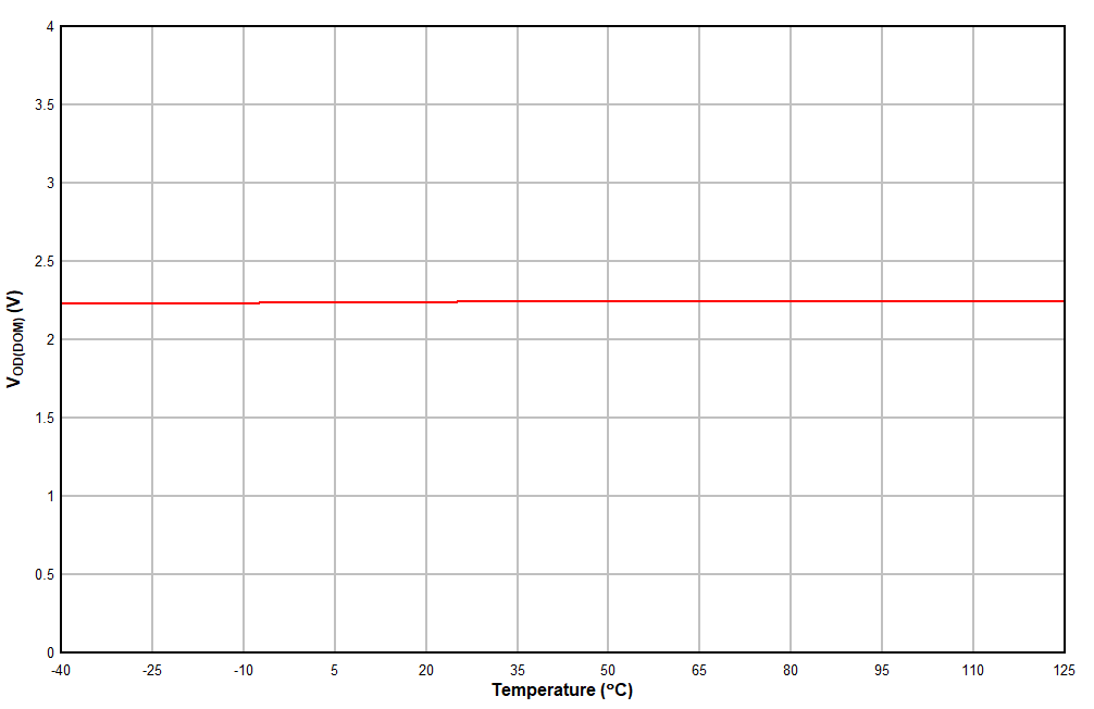
| VCC = 5V | VIO = 3.3V | RL = 60Ω |
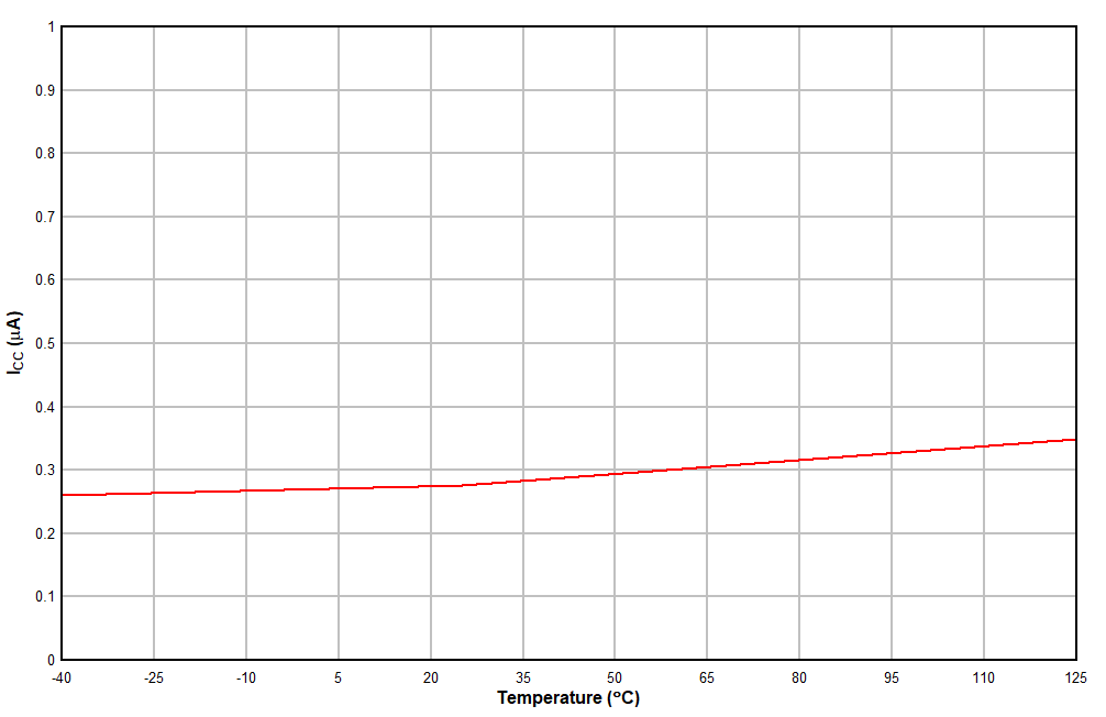
| VCC = 5V | VIO = 3.3V | RL = 60Ω |
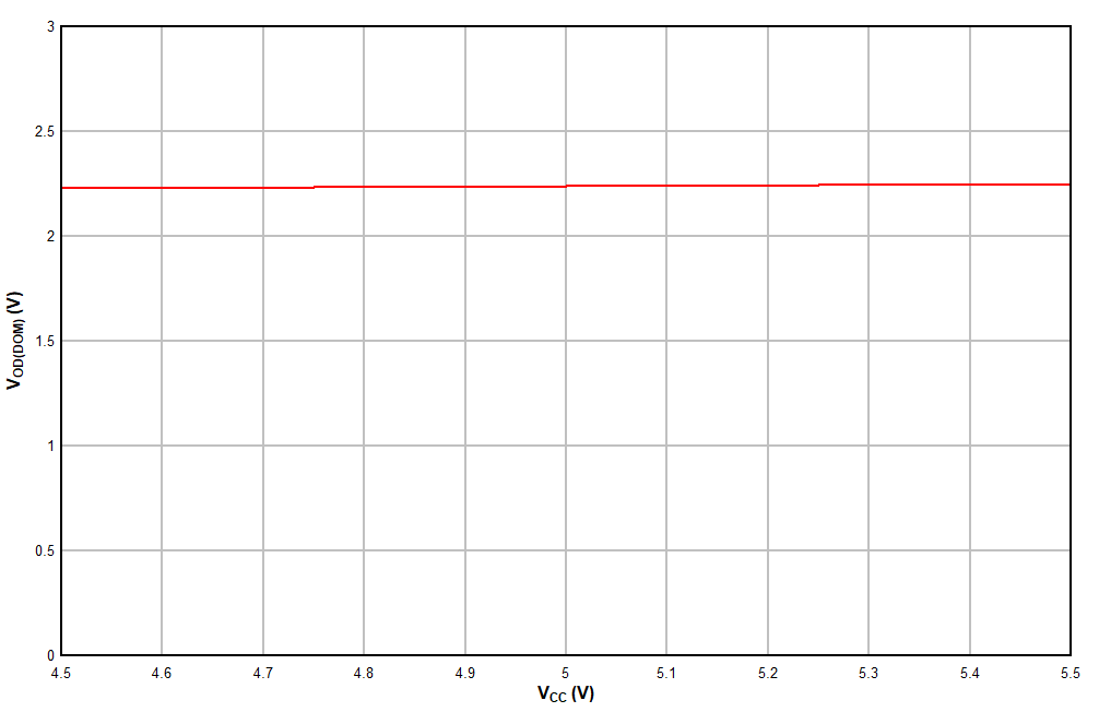
| Temp = 25°C | RL = 60Ω |
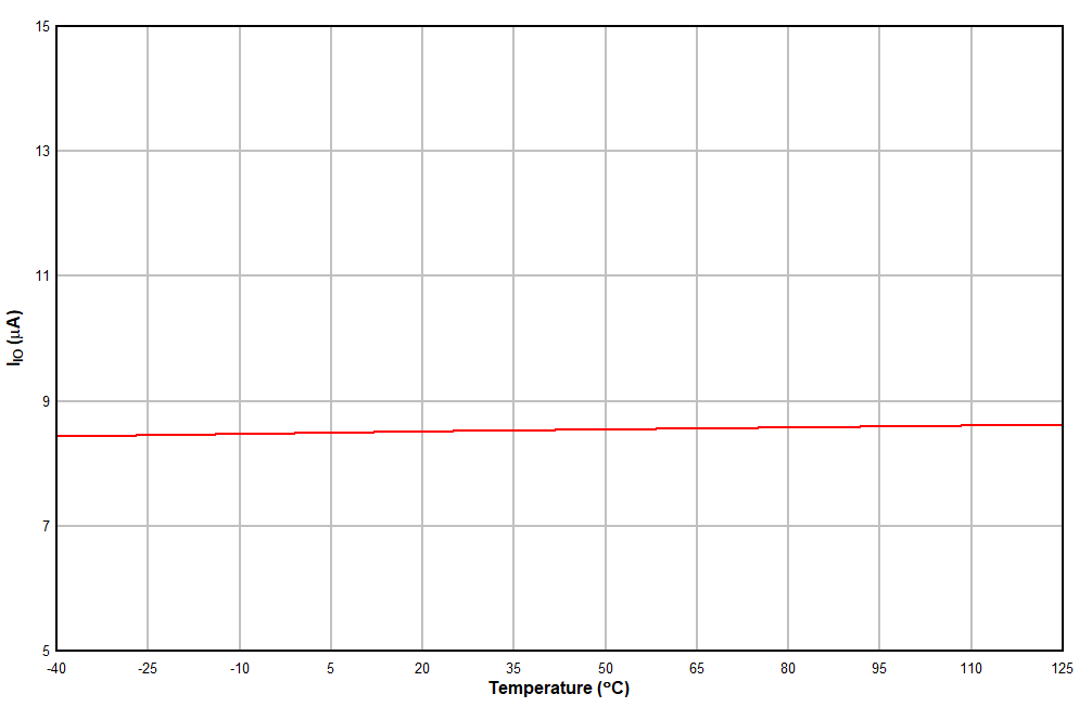
| VCC = 5V | VIO = 3.3V | RL = 60Ω |
6 Parameter Measurement Information
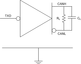 Figure 6-1 ICC Test Circuit
 Figure 6-2 Driver Test Circuit and Measurement
 Figure 6-3 Receiver Test Circuit and Measurement
| Input (See Figure 6-3) | Output | |||
|---|---|---|---|---|
| VCANH | VCANL | |VID| | RXD | |
| -11.5V | -12.5V | 1000mV | Low | VOL |
| 12.5V | 11.5V | 1000mV | ||
| -8.55V | -9.45V | 900mV | ||
| 9.45 V | 8.55V | 900mV | ||
| -8.75V | -9.25V | 500mV | High | VOH |
| 9.25V | 8.75V | 500mV | ||
| -11.8 V | -12.2V | 400mV | ||
| 12.2V | 11.8V | 400mV | ||
| Open | Open | X | ||
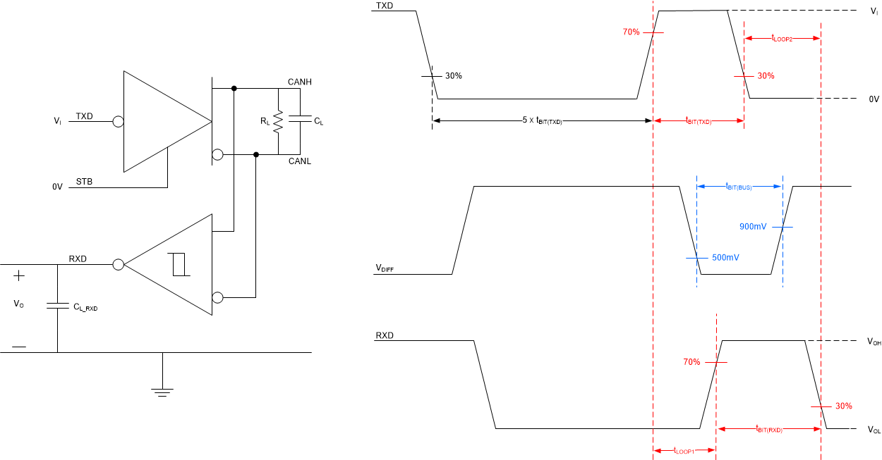 Figure 6-4 Transmitter and Receiver Timing Test Circuit and
Measurement
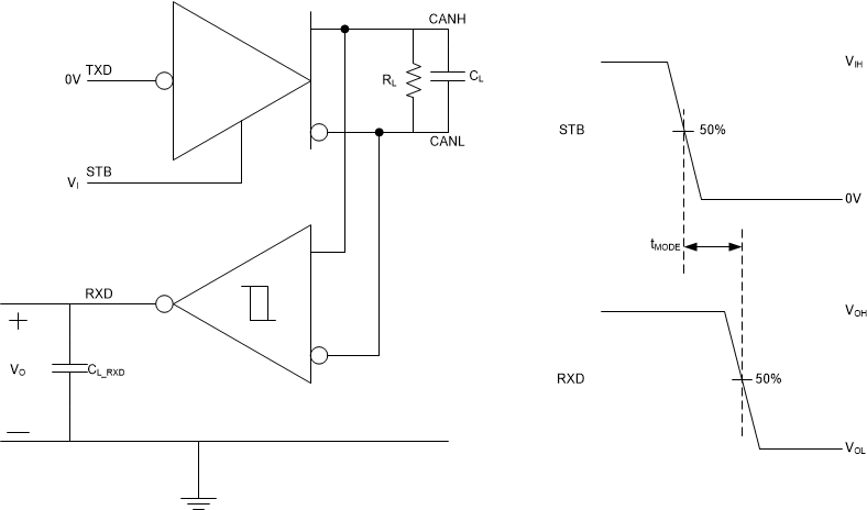 Figure 6-5 tMODE Test Circuit and
Measurement
 Figure 6-6 TXD
Dominant Timeout Test Circuit and
Measurement
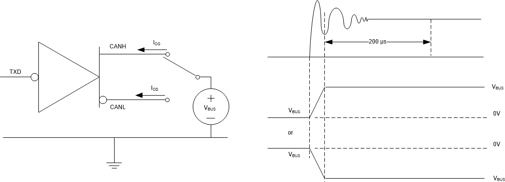 Figure 6-7 Driver Short-Circuit Current Test and
Measurement
Figure 6-7 Driver Short-Circuit Current Test and
Measurement7 Detailed Description
7.1 Overview
The TCAN1044-Q1 meets or exceeds the specifications of the ISO 11898-2:2016 high speed CAN (Controller Area Network) physical layer standard. The device has been certified to the requirements of ISO 11898-2:2016 and ISO 11898-5:2007 physical layer requirements according to the GIFT/ICT high speed CAN test specification. The transceiver provides a number of different protection features making it ideal for the stringent automotive system requirements while also supporting CAN FD data rates up to 8Mbps.
The TCAN1044-Q1 conforms to the following CAN standards:
- CAN transceiver physical layer standards:
- ISO 11898-2:2016 High speed medium access unit
- ISO 11898-5:2007 High speed medium access unit with low-power mode
- SAE J2284-1: High Speed CAN (HSC) for Vehicle Applications at 125kbps
- SAE J2284-2: High Speed CAN (HSC) for Vehicle Applications at 250kbps
- SAE J2284-3: High Speed CAN (HSC) for Vehicle Applications at 500kbps
- SAE J2284-4: High-Speed CAN (HSC) for Vehicle Applications at 500kbps with CAN FD Data at 2Mbps
- SAE J2284-5: High-Speed CAN (HSC) for Vehicle Applications at 500kbps with CAN FD Data at 5Mbps
- ARINC 825-4 General Standardization of CAN (Controller Area Network) Bus Protocol For Airborne Use
- EMC requirements:
- VeLIO (Vehicle LAN Interoperability and Optimization) CAN and CAN-FD Transceiver Requirements
- SAE J2962-2 Communication Transceivers Qualification Requirements – CAN
- Conformance test requirements:
- ISO 16845-2 Road vehicles – Controller area network (CAN) conformance test plan Part 2: High-speed medium access unit conformance test plan
7.2 Functional Block Diagram
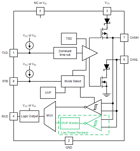 Figure 7-1 Block Diagram
7.3 Feature Description
7.3.1 Pin Description
7.3.1.1 TXD
The TXD input is a logic-level signal, referenced to either VCC or VIO from a CAN controller to the TCAN1044-Q1 transceivers.
7.3.1.2 GND
GND is the ground pin of the transceiver, it must be connected to the PCB ground.
7.3.1.3 VCC
VCC provides the 5V power supply to the CAN transceiver.
7.3.1.4 RXD
The RXD output is a logic-level signal, referenced to either VCC or VIO, from the TCAN1044-Q1 transceivers to the CAN controller. RXD is only driven once VIO is present.
When a wake event takes place RXD is driven low.
7.3.1.5 VIO
The VIO pin provides the digital I/O voltage to match the CAN controller voltage thus avoiding the requirement for a level shifter. It supports voltages from 1.7V to 5.5V providing the widest range of controller support.
7.3.1.6 CANH and CANL
These are the CAN high and CAN low differential bus pins. These pins are connected to the CAN transceiver and the low-voltage WUP CAN receiver.
7.3.1.7 STB (Standby)
The STB pin is an input pin used for mode control of the transceiver. The STB pin can be supplied from either the system processor or from a static system voltage source. If normal mode is the only intended mode of operation, then the STB pin can be tied directly to GND.
7.3.2 CAN Bus States
The CAN bus has two logical states during operation: recessive and dominant. See Figure 7-2 and Figure 7-3.
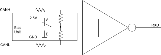
A dominant bus state occurs when the bus is driven differentially and corresponds to a logic low on the TXD and RXD pins. A recessive bus state occurs when the bus is biased to VCC/2 via the high-resistance internal input resistors RIN) of the receiver and corresponds to a logic high on the TXD and RXD pins.
A dominant state overwrites the recessive state during arbitration. Multiple CAN nodes may be transmitting a dominant bit at the same time during arbitration, and in this case the differential voltage of the bus is greater than the differential voltage of a single driver.
The TCAN1044-Q1 transceiver implements a low-power standby (STB) mode which enables a third bus state where the bus pins are weakly biased to ground via the high resistance internal resistors of the receiver. See Figure 7-2 and Figure 7-3.
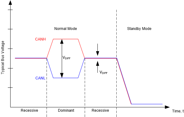 Figure 7-2 Bus States
7.3.3 TXD Dominant Timeout (DTO)
During normal mode, the only mode where the CAN driver is active, the TXD DTO circuit prevents the local node from blocking network communication in the event of a hardware or software failure where TXD is held dominant longer than the timeout period tTXD_DTO. The TXD DTO circuit is triggered by a falling edge on TXD. If no rising edge is seen before the timeout period of the circuit, tTXD_DTO, the CAN driver is disabled. This frees the bus for communication between other nodes on the network. The CAN driver is reactivated when a recessive signal is seen on the TXD pin, thus clearing the dominant timeout. The receiver remains active and biased to VCC/2 and the RXD output reflects the activity on the CAN bus during the TXD DTO fault.
The minimum dominant TXD time allowed by the TXD DTO circuit limits the minimum possible transmitted data rate of the device. The CAN protocol allows a maximum of eleven successive dominant bits (on TXD) for the worst case, where five successive dominant bits are followed immediately by an error frame. The minimum transmitted data rate may be calculated using Equation 1.
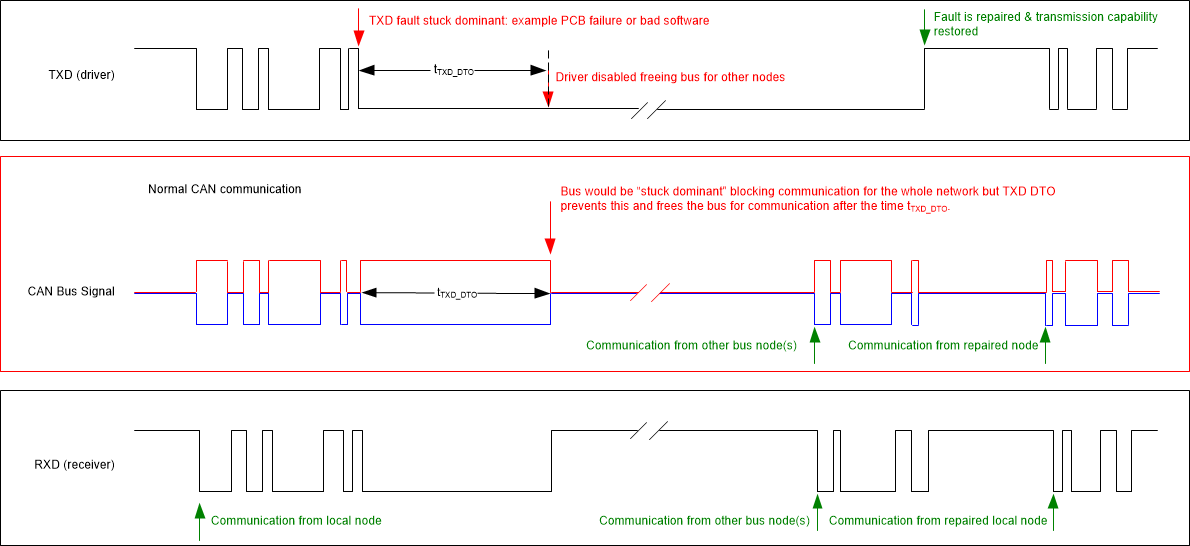 Figure 7-4 Example Timing Diagram for TXD Dominant Timeout
7.3.4 CAN Bus Short Circuit Current Limiting
The TCAN1044-Q1 has several protection features that limit the short circuit current when a CAN bus line is shorted. These include CAN driver current limiting in the dominant and recessive states and TXD dominant state timeout which prevents permanently having the higher short circuit current of a dominant state in case of a system fault. During CAN communication the bus switches between the dominant and recessive states, thus the short circuit current may be viewed as either the current during each bus state or as a DC average current. When selecting termination resistors or a common mode choke for the CAN design the average power rating, IOS(AVG), should be used. The percentage dominant is limited by the TXD DTO and the CAN protocol which has forced state changes and recessive bits due to bit stuffing, control fields, and interframe space. These ensure there is a minimum amount of recessive time on the bus even if the data field contains a high percentage of dominant bits.
The average short circuit current of the bus depends on the ratio of recessive to dominant bits and their respective short circuit currents. The average short circuit current may be calculated using 2.
Where:
- IOS(AVG) is the average short circuit current
- % Transmit is the percentage the node is transmitting CAN messages
- % Receive is the percentage the node is receiving CAN messages
- % REC_Bits is the percentage of recessive bits in the transmitted CAN messages
- % DOM_Bits is the percentage of dominant bits in the transmitted CAN messages
- IOS(SS)_REC is the recessive steady state short circuit current
- IOS(SS)_DOM is the dominant steady state short circuit current
This short circuit current and the possible fault cases of the network should be taken into consideration when sizing the power supply used to generate the transceivers VCC supply.
7.3.5 Thermal Shutdown (TSD)
If the junction temperature of the TCAN1044-Q1 exceeds the thermal shutdown threshold, TTSD, the device turns off the CAN driver circuitry and blocks the TXD to bus transmission path. The shutdown condition is cleared when the junction temperature of the device drops below TTSD. The CAN bus pins are biased to VCC/2 during a TSD fault and the receiver to RXD path remains operational. The TCAN1044-Q1 TSD circuit includes hysteresis which prevents the CAN driver output from oscillating during a TSD fault.
7.3.6 Undervoltage Lockout
The supply pins, VCC and VIO, have undervoltage detection that places the device into a protected state. This protects the bus during an undervoltage event on either supply pin.
| VCC | DEVICE STATE | BUS | RXD PIN |
|---|---|---|---|
| > UVVCC | Normal | Per TXD | Mirrors bus |
| < UVVCC | Protected | High impedance Weak pull-down to ground(1) | High impedance |
| VCC | VIO | DEVICE STATE | BUS | RXD PIN |
|---|---|---|---|---|
| > UVVCC | > UVVIO | Normal | Per TXD | Mirrors bus |
| < UVVCC | > UVVIO | STB = VIO: standby mode | High impedance Weak pull-down to ground(1) | VIO: Remote wake request(2) |
| STB = GND: Protected | Recessive | |||
| > UVVCC | < UVVIO | Protected | High impedance | |
| < UVVCC | < UVVIO | Protected | High impedance |
Once the undervoltage condition is cleared and tMODE has expired the TCAN1044-Q1 transitions to normal mode and the host controller can send and receive CAN traffic again.
7.3.7 Unpowered Device
The TCAN1044-Q1 is designed to be an ideal passive or no load to the CAN bus if the device is unpowered. The bus pins were designed to have low leakage currents when the device is unpowered, so they do not load the bus. This is critical if some nodes of the network are unpowered while the rest of the of network remains operational.
The logic pins also have low leakage currents when the device is unpowered, so they do not load other circuits which may remain powered.
7.3.8 Floating pins
The TCAN1044-Q1 has internal pull-ups on critical pins which place the device into known states if the pin floats. This internal bias should not be relied upon by design though, especially in noisy environments, but instead should be considered a failsafe protection feature.
When a CAN controller supporting open-drain outputs is used an adequate external pull-up resistor must be chosen. This makes sure the TXD output of the CAN controller maintains acceptable bit time to the input of the CAN transceiver. See Table 7-3 for details on pin bias conditions.
| Pin | Pull-up or Pull-down | Comment |
|---|---|---|
| TXD | Pull-up | Weakly biases TXD towards recessive to prevent bus blockage or TXD DTO triggering |
| STB | Pull-up | Weakly biases STB towards low-power standby mode to prevent excessive system power |
7.4 Device Functional Modes
7.4.1 Operating Modes
The TCAN1044-Q1 has two main operating modes: normal mode and standby mode. Operating mode selection is made by applying a high or low level to the STB pin on the TCAN1044-Q1.
| STB | Device Mode | Driver | Receiver | RXD Pin |
|---|---|---|---|---|
| High | Low current standby mode with bus wake-up | Disabled | Low-power receiver and bus monitor enable | High (recessive) until valid WUP is received See Section 7.4.3.1 |
| Low | Normal Mode | Enabled | Enabled | Mirrors bus state |
7.4.2 Normal Mode
This is the normal operating mode of the TCAN1044-Q1. The CAN driver and receiver are fully operational and CAN communication is bi-directional. The driver is translating a digital input on the TXD input to a differential output on the CANH and CANL bus pins. The receiver is translating the differential signal from CANH and CANL to a digital output on the RXD output.
7.4.3 Standby Mode
This is the low-power mode of the TCAN1044-Q1. The CAN driver and main receiver are switched off and bi-directional CAN communication is not possible. The low-power receiver and bus monitor circuits are enabled to allow for RXD wake-up requests via the CAN bus. A wake-up request is output to RXD as shown in Figure 7-5. The local CAN protocol controller should monitor RXD for transitions (high-to-low) and reactivate the device to normal mode by pulling the STB pin low. The CAN bus pins are weakly pulled to GND in this mode; see Figure 7-2 and Figure 7-3.
In standby mode, only the VIO supply is required therefore the VCC may be switched off for additional system level current savings.