JAJSG75B September 2018 – April 2024 LM5164-Q1
PRODUCTION DATA
- 1
- 1 特長
- 2 アプリケーション
- 3 概要
- 4 Pin Configuration and Functions
- 5 Specifications
-
6 Detailed Description
- 6.1 Overview
- 6.2 Functional Block Diagram
- 6.3
Feature Description
- 6.3.1 Control Architecture
- 6.3.2 Internal VCC Regulator and Bootstrap Capacitor
- 6.3.3 Regulation Comparator
- 6.3.4 Internal Soft Start
- 6.3.5 On-Time Generator
- 6.3.6 Current Limit
- 6.3.7 N-Channel Buck Switch and Driver
- 6.3.8 Synchronous Rectifier
- 6.3.9 Enable/Undervoltage Lockout (EN/UVLO)
- 6.3.10 Power Good (PGOOD)
- 6.3.11 Thermal Protection
- 6.4 Device Functional Modes
- 7 Application and Implementation
- 8 Device and Documentation Support
- 9 Revision History
- 10Mechanical, Packaging, and Orderable Information
6.3.6 Current Limit
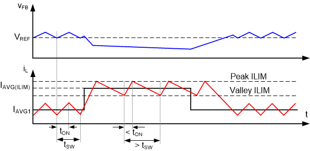
The LM5164-Q1 manages overcurrent conditions with cycle-by-cycle current limiting of the peak inductor current. The current sensed in the high-side MOSFET is compared every switching cycle to the current limit threshold (1.5 A). To protect the converter from potential current runaway conditions, the LM5164-Q1 includes a foldback valley current limit feature, set at 1.2 A, that is enabled if a peak current limit is detected. As shown in Figure 6-1, if the peak current in the high-side MOSFET exceeds 1.5 A (typical), the present cycle is immediately terminated regardless of the programmed on-time (tON), the high-side MOSFET is turned off and the foldback valley current limit is activated. The low-side MOSFET remains on until the inductor current drops below this foldback valley current limit, after which the next on-pulse is initiated. This method folds back the switching frequency to prevent overheating and limits the average output current to less than 1.5 A to ensure proper short-circuit and heavy-load protection of the LM5164-Q1.
 Figure 6-1 Current Limit Timing Diagram
Current is sensed after a leading-edge blanking time following the high-side MOSFET turnon transition. The propagation delay of the current limit comparator is 100 ns. During high step-down conditions when the on-time is less than 100 ns, a back-up peak current limit comparator in the low-side FET also set at 1.5 A enables the foldback valley current limit set at 1.2 A. This innovative current limit scheme enables ultra-low duty-cycle operation, permitting large step-down voltage conversions while ensuring robust protection of the converter.