JAJSGO4D November   2018  – December 2019 TPS1HA08-Q1

PRODUCTION DATA.  

  1. 特長
  2. アプリケーション
  3. 概要
    1.     概略回路図
  4. 改訂履歴
  5. Device Comparison Table
  6. Pin Configuration and Functions
    1.     Pin Functions
    2. 6.1 Recommended Connections for Unused Pins
  7. Specifications
    1. 7.1 Absolute Maximum Ratings
    2. 7.2 ESD Ratings
    3. 7.3 Recommended Operating Conditions
    4. 7.4 Thermal Information
    5. 7.5 Electrical Characteristics
    6. 7.6 Switching Characteristics
    7. 7.7 SNS Timing Characteristics
    8. 7.8 Typical Characteristics
  8. Parameter Measurement Information
  9. Detailed Description
    1. 9.1 Overview
      1. 9.1.1 Device Nomenclature
    2. 9.2 Functional Block Diagram
    3. 9.3 Feature Description
      1. 9.3.1 Protection Mechanisms
        1. 9.3.1.1 Thermal Shutdown
        2. 9.3.1.2 Current Limit
          1. 9.3.1.2.1 Current Limit Foldback
          2. 9.3.1.2.2 Selectable Current Limit Threshold
          3. 9.3.1.2.3 Undervoltage Lockout (UVLO)
          4. 9.3.1.2.4 VBB during Short-to-Ground
        3. 9.3.1.3 Energy Limit
        4. 9.3.1.4 Voltage Transients
          1. 9.3.1.4.1 Load Dump
          2. 9.3.1.4.2 Driving Inductive and Capacitive Loads
        5. 9.3.1.5 Reverse Battery
        6. 9.3.1.6 Fault Event – Timing Diagrams
      2. 9.3.2 Diagnostic Mechanisms
        1. 9.3.2.1 VOUT Short-to-Battery and Open-Load
          1. 9.3.2.1.1 Detection With Switch Enabled
          2. 9.3.2.1.2 Detection With Switch Disabled
        2. 9.3.2.2 SNS Output
          1. 9.3.2.2.1 RSNS Value
            1. 9.3.2.2.1.1 High Accuracy Load Current Sense
            2. 9.3.2.2.1.2 SNS Output Filter
        3. 9.3.2.3 ST Pin
        4. 9.3.2.4 Fault Indication and SNS Mux
        5. 9.3.2.5 Resistor Sharing
        6. 9.3.2.6 High-Frequency, Low Duty-Cycle Current Sensing
      3. 9.3.3 Enable Watchdog
    4. 9.4 Device Functional Modes
      1. 9.4.1 Off
      2. 9.4.2 Standby
      3. 9.4.3 Diagnostic
      4. 9.4.4 Standby Delay
      5. 9.4.5 Active
      6. 9.4.6 Fault
  10. 10Application and Implementation
    1. 10.1 Application Information
      1. 10.1.1 Ground Protection Network
      2. 10.1.2 Interface With Microcontroller
      3. 10.1.3 I/O Protection
      4. 10.1.4 Inverse Current
      5. 10.1.5 Loss of GND
      6. 10.1.6 Automotive Standards
        1. 10.1.6.1 ISO7637-2
        2. 10.1.6.2 AEC – Q100-012 Short Circuit Reliability
      7. 10.1.7 Thermal Information
    2. 10.2 Typical Application
      1. 10.2.1 Design Requirements
      2. 10.2.2 Detailed Design Procedure
        1. 10.2.2.1 Thermal Considerations
        2. 10.2.2.2 Diagnostics
          1. 10.2.2.2.1 Selecting the RISNS Value
      3. 10.2.3 Application Curves
  11. 11Power Supply Recommendations
  12. 12Layout
    1. 12.1 Layout Guidelines
    2. 12.2 Layout Example
  13. 13デバイスおよびドキュメントのサポート
    1. 13.1 デバイス・サポート
      1. 13.1.1 関連資料
    2. 13.2 商標
    3. 13.3 静電気放電に関する注意事項
    4. 13.4 Glossary
  14. 14メカニカル、パッケージ、および注文情報

Reverse Battery

In the reverse battery condition, the switch will automatically be enabled (regardless of EN status) to prevent power dissipation inside the MOSFET body diode. In many applications (for example, resistive load), the full load current may be present during reverse battery. In order to activate the automatic switch on feature, the SEL2 pin must have a path to module ground. This may be path 1 as shown below, or, if the SEL2 pin is unused, the path may be through RPROT to module ground.

Protection features (for example, thermal shutdown) are not available during reverse battery. Care must be taken to ensure that excessive power is not dissipated in the switch during the reverse battery condition.

There are two options for blocking reverse current in the system. Option 1 is to place a blocking device (FET or diode) in series with the battery supply. This will block all current paths. Option 2 is to place a blocking diode in series with the GND node of the high-side switch. This method will protect the controller portion of the switch (path 2), but it will not prevent current from flowing through the load (path 3). The diode used for Option 2 may be shared amongst multiple high-side switches.

Path 1 shown in Figure 41 is blocked inside of the device.
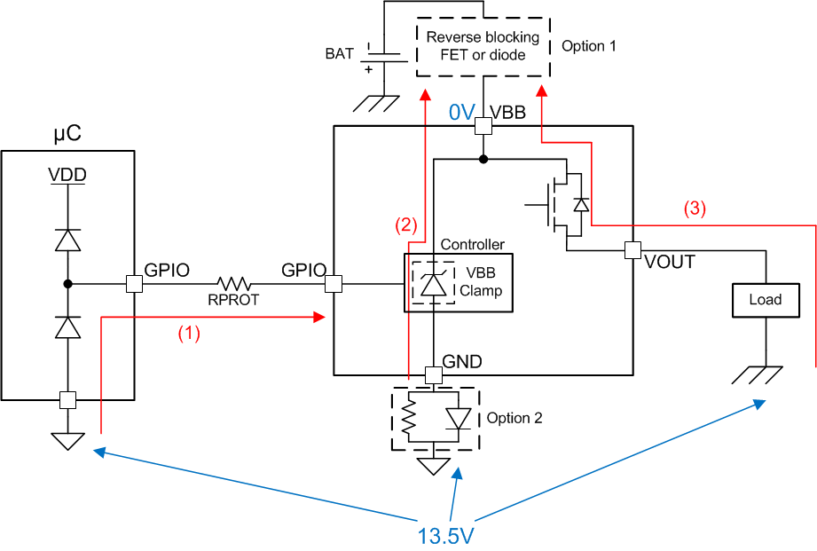
TPS1HA08-Q1 reverse_batt_slvsd84.gifFigure 41. Current Path During Reverse Battery