JAJSGO8F July   2013  – February 2020 TAS5760M

PRODUCTION DATA.  

  1. 特長
  2. アプリケーション
  3. 概要
    1.     Device Images
      1.      機能ブロック図
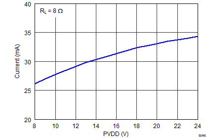
      2.      10% THD+Nでの電力とPVDDとの関係
  4. 改訂履歴
  5. Pin Configuration and Functions
    1.     Pin Functions
    2.     Pin Functions
  6. Specifications
    1. 6.1  Absolute Maximum Ratings
    2. 6.2  ESD Ratings
    3. 6.3  Recommended Operating Conditions
    4. 6.4  Digital I/O Pins
    5. 6.5  Master Clock
    6. 6.6  Serial Audio Port
    7. 6.7  Protection Circuitry
    8. 6.8  Speaker Amplifier in All Modes
    9. 6.9  Speaker Amplifier in Stereo Bridge Tied Load (BTL) Mode
    10. 6.10 Speaker Amplifier in Mono Parallel Bridge Tied Load (PBTL) Mode
    11. 6.11 I²C Control Port
    12. 6.12 Typical Idle, Mute, Shutdown, Operational Power Consumption
    13. 6.13 Typical Characteristics (Stereo BTL Mode): fSPK_AMP = 384 kHz
    14. 6.14 Typical Characteristics (Stereo BTL Mode): fSPK_AMP = 768 kHz
    15. 6.15 Typical Characteristics (Mono PBTL Mode): fSPK_AMP = 384 kHz
    16. 6.16 Typical Characteristics (Mono PBTL Mode): fSPK_AMP = 768 kHz
  7. Parameter Measurement Information
  8. Detailed Description
    1. 8.1 Overview
    2. 8.2 Functional Block Diagram
      1. 8.2.1 Functional Block Diagram
    3. 8.3 Feature Description
      1. 8.3.1 Power Supplies
      2. 8.3.2 Speaker Amplifier Audio Signal Path
        1. 8.3.2.1 Serial Audio Port (SAP)
          1. 8.3.2.1.1 I²S Timing
          2. 8.3.2.1.2 Left-Justified
          3. 8.3.2.1.3 Right-Justified
        2. 8.3.2.2 DC Blocking Filter
        3. 8.3.2.3 Digital Boost and Volume Control
        4. 8.3.2.4 Digital Clipper
        5. 8.3.2.5 Closed-Loop Class-D Amplifier
      3. 8.3.3 Speaker Amplifier Protection Suite
        1. 8.3.3.1 Speaker Amplifier Fault Notification (SPK_FAULT Pin)
        2. 8.3.3.2 DC Detect Protection
    4. 8.4 Device Functional Modes
      1. 8.4.1 Hardware Control Mode
        1. 8.4.1.1 Speaker Amplifier Shut Down (SPK_SD Pin)
        2. 8.4.1.2 Serial Audio Port in Hardware Control Mode
        3. 8.4.1.3 Soft Clipper Control (SFT_CLIP Pin)
        4. 8.4.1.4 Speaker Amplifier Switching Frequency Select (FREQ/SDA Pin)
        5. 8.4.1.5 Parallel Bridge Tied Load Mode Select (PBTL/SCL Pin)
        6. 8.4.1.6 Speaker Amplifier Sleep Enable (SPK_SLEEP/ADR Pin)
        7. 8.4.1.7 Speaker Amplifier Gain Select (SPK_GAIN [1:0] Pins)
        8. 8.4.1.8 Considerations for Setting the Speaker Amplifier Gain Structure
          1. 8.4.1.8.1 Recommendations for Setting the Speaker Amplifier Gain Structure in Hardware Control Mode
      2. 8.4.2 Software Control Mode
        1. 8.4.2.1 Speaker Amplifier Shut Down (SPK_SD Pin)
        2. 8.4.2.2 Serial Audio Port Controls
          1. 8.4.2.2.1 Serial Audio Port (SAP) Clocking
        3. 8.4.2.3 Parallel Bridge Tied Load Mode via Software Control
        4. 8.4.2.4 Speaker Amplifier Gain Structure
          1. 8.4.2.4.1 Speaker Amplifier Gain in Software Control Mode
          2. 8.4.2.4.2 Considerations for Setting the Speaker Amplifier Gain Structure
          3. 8.4.2.4.3 Recommendations for Setting the Speaker Amplifier Gain Structure in Software Control Mode
        5. 8.4.2.5 I²C Software Control Port
          1. 8.4.2.5.1 Setting the I²C Device Address
          2. 8.4.2.5.2 General Operation of the I²C Control Port
          3. 8.4.2.5.3 Writing to the I²C Control Port
          4. 8.4.2.5.4 Reading from the I²C Control Port
    5. 8.5 Register Maps
      1. 8.5.1 Control Port Registers - Quick Reference
      2. 8.5.2 Control Port Registers - Detailed Description
        1. 8.5.2.1  Device Identification Register (0x00)
          1. Table 9. Device Identification Register Field Descriptions
        2. 8.5.2.2  Power Control Register (0x01)
          1. Table 10. Power Control Register Field Descriptions
        3. 8.5.2.3  Digital Control Register (0x02)
          1. Table 11. Digital Control Register Field Descriptions
        4. 8.5.2.4  Volume Control Configuration Register (0x03)
          1. Table 12. Volume Control Configuration Register Field Descriptions
        5. 8.5.2.5  Left Channel Volume Control Register (0x04)
          1. Table 13. Left Channel Volume Control Register Field Descriptions
        6. 8.5.2.6  Right Channel Volume Control Register (0x05)
          1. Table 14. Right Channel Volume Control Register Field Descriptions
        7. 8.5.2.7  Analog Control Register (0x06)
          1. Table 15. Analog Control Register Field Descriptions
        8. 8.5.2.8  Reserved Register (0x07)
        9. 8.5.2.9  Fault Configuration and Error Status Register (0x08)
          1. Table 16. Fault Configuration and Error Status Register Field Descriptions
        10. 8.5.2.10 Reserved Controls (9 / 0x09) - (15 / 0x0F)
        11. 8.5.2.11 Digital Clipper Control 2 Register (0x10)
          1. Table 17. Digital Clipper Control 2 Register Field Descriptions
        12. 8.5.2.12 Digital Clipper Control 1 Register (0x11)
          1. Table 18. Digital Clipper Control 1 Register Field Descriptions
  9. Application and Implementation
    1. 9.1 Application Information
    2. 9.2 Typical Applications
      1. 9.2.1 Stereo BTL Using Software Control
        1. 9.2.1.1 Design Requirements
        2. 9.2.1.2 Detailed Design Procedure
          1. 9.2.1.2.1 Startup Procedures- Software Control Mode
          2. 9.2.1.2.2 Shutdown Procedures- Software Control Mode
          3. 9.2.1.2.3 Component Selection and Hardware Connections
            1. 9.2.1.2.3.1 I²C Pullup Resistors
            2. 9.2.1.2.3.2 Digital I/O Connectivity
          4. 9.2.1.2.4 Recommended Startup and Shutdown Procedures
        3. 9.2.1.3 Application Curves
      2. 9.2.2 Stereo BTL Using Software Control, 32-Pin DAP Package Option
        1. 9.2.2.1 Design Requirements
        2. 9.2.2.2 Detailed Design Procedure
          1. 9.2.2.2.1 Startup Procedures- Software Control Mode
          2. 9.2.2.2.2 Shutdown Procedures- Software Control Mode
          3. 9.2.2.2.3 Component Selection and Hardware Connections
            1. 9.2.2.2.3.1 I²C Pullup Resistors
            2. 9.2.2.2.3.2 Digital I/O Connectivity
          4. 9.2.2.2.4 Recommended Startup and Shutdown Procedures
        3. 9.2.2.3 Application Curve
      3. 9.2.3 Stereo BTL Using Hardware Control, 32-Pin DAP Package Option
        1. 9.2.3.1 Design Requirements
        2. 9.2.3.2 Detailed Design Procedure
          1. 9.2.3.2.1 Startup Procedures - Hardware Control Mode
          2. 9.2.3.2.2 Shutdown Procedures - Hardware Control Mode
          3. 9.2.3.2.3 Digital I/O Connectivity
        3. 9.2.3.3 Application Curve
      4. 9.2.4 Mono PBTL Using Software Control, 32-Pin DAP Package Option
        1. 9.2.4.1 Design Requirements
        2. 9.2.4.2 Detailed Design Procedure
          1. 9.2.4.2.1 Startup Procedures - Software Control Mode
          2. 9.2.4.2.2 Shutdown Procedures - Software Control Mode
          3. 9.2.4.2.3 Component Selection and Hardware Connections
            1. 9.2.4.2.3.1 I²C Pull-Up Resistors
            2. 9.2.4.2.3.2 Digital I/O Connectivity
              1. 9.2.4.2.3.2.1 Application Curves
      5. 9.2.5 Mono PBTL Using Hardware Control, 32-Pin DAP Package Option
        1. 9.2.5.1 Design Requirements
        2. 9.2.5.2 Detailed Design Procedure
          1. 9.2.5.2.1 Startup Procedures - Hardware Control Mode
          2. 9.2.5.2.2 Shutdown Procedures - Hardware Control Mode
          3. 9.2.5.2.3 Digital I/O Connectivity
          4. 9.2.5.2.4 Application Curves
  10. 10Power Supply Recommendations
    1. 10.1 DVDD Supply
    2. 10.2 PVDD Supply
  11. 11Layout
    1. 11.1 Layout Guidelines
      1. 11.1.1 General Guidelines for Audio Amplifiers
      2. 11.1.2 Importance of PVDD Bypass Capacitor Placement on PVDD Network
      3. 11.1.3 Optimizing Thermal Performance
        1. 11.1.3.1 Device, Copper, and Component Layout
        2. 11.1.3.2 Stencil Pattern
          1. 11.1.3.2.1 PCB Footprint and Via Arrangement
            1. 11.1.3.2.1.1 Solder Stencil
    2. 11.2 Layout Example
  12. 12デバイスおよびドキュメントのサポート
    1. 12.1 ドキュメントのサポート
      1. 12.1.1 関連資料
    2. 12.2 サポート・リソース
    3. 12.3 商標
    4. 12.4 静電気放電に関する注意事項
    5. 12.5 Glossary
  13. 13メカニカル、パッケージ、および注文情報

Typical Characteristics (Stereo BTL Mode): fSPK_AMP = 384 kHz

At TA = 25°C, fSPK_AMP = 384 kHz, input signal is 1 kHz Sine, unless otherwise noted. Filter used for 8 Ω = 22 µH + 0.68 µF, Filter used for 6 Ω = 15 µH + 0.68 µF, Filter used for 4 Ω = 10 µH + 0.68 µF unless otherwise noted.
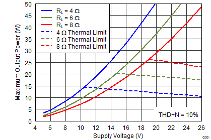
TAS5760M G001_SLOS741.png
Thermal Limits are referenced to TAS5760xxEVM Rev D
Figure 1. Output Power vs PVDD
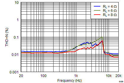
TAS5760M G025_THDvsF_24V.png
PVDD = 24 V, POSPK = 1 W
Figure 3. THD+N vs Frequency
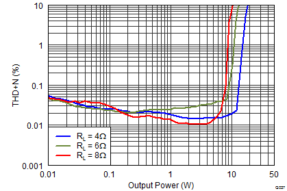
TAS5760M G027_THDN_vs_Po_12V_1000.png
PVDD = 12 V, Both Channels Driven
Figure 5. THD+N vs Output Power
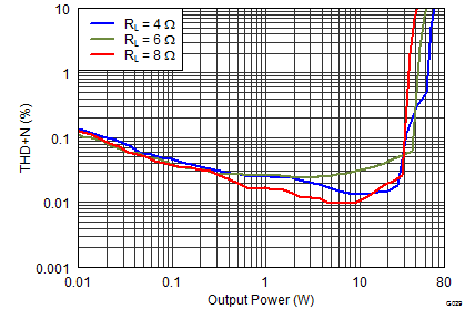
TAS5760M G029_THDN_vs_Po_24V_1000.png
PVDD = 24 V, Both Channels Driven
Figure 7. THD+N vs Output Power
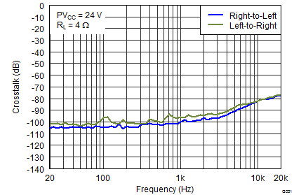
TAS5760M G031_XTalkvFreq_24V_4R.pngFigure 9. Crosstalk vs Frequency
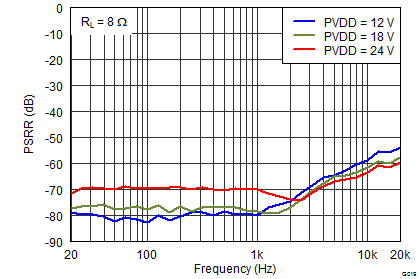
TAS5760M G020_SLOS741.pngFigure 11. DVDD PSRR vs Frequency
TAS5760M G023_Idle_Current_PVDD_LCFilter_384_BTL.png
With LC Filter as Shown on the EVM
Figure 13. Idle Current Draw vs PVDD
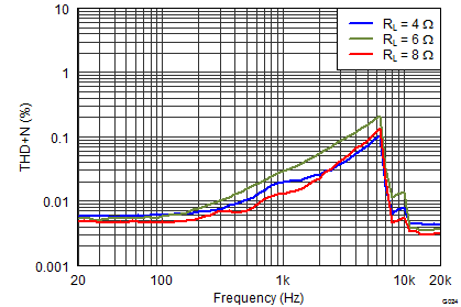
TAS5760M G024_THDvsF_12V.png
PVDD = 12 V, POSPK = 1 W
Figure 2. THD+N vs Frequency
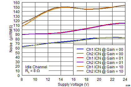
TAS5760M G026_BTL_ICNvsPVcc_8R.pngFigure 4. Idle Channel Noise vs PVDD
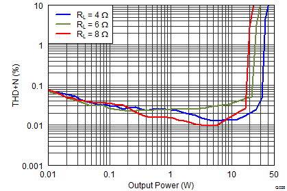
TAS5760M G028_THDN_vs_Po_18V_1000.png
PVDD = 18 V, Both Channels Driven
Figure 6. THD+N vs Output Power
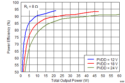
TAS5760M G030_EffvPo_12V_18V_24V_8R.pngFigure 8. Efficiency vs Output Power
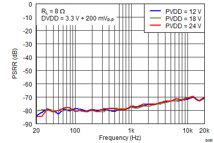
TAS5760M G019_SLOS741.pngFigure 10. PVDD PSRR vs Frequency
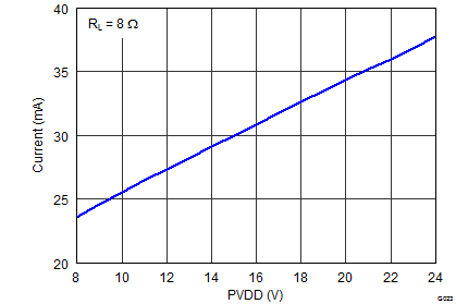
TAS5760M G042_Idle_Current_PVDD_Filterless_384_BTL.pngFigure 12. Idle Current Draw vs PVDD (Filterless)
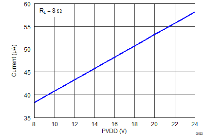
TAS5760M G022_Idle_Current_PVDD_Shutdown_8R.pngFigure 14. Shutdown Current Draw vs PVDD (Filterless)