JAJSGS3B January 2019 – July 2022 ADS8353-Q1
PRODUCTION DATA
- 1特長
- 2アプリケーション
- 3概要
- 4Revision History
- 5Pin Configuration and Functions
- 6Specifications
- 7Detailed Description
- 8Application and Implementation
- 9Device and Documentation Support
7.5.3.2.2 32-CLK, Single-SDO Mode (CFR.B11 = 0, CFR.B10 = 1)
The 32-CLK, single-SDO mode provides the option of using only one SDO pin (SDO_A) to read conversion results from both ADCs (ADC_A and ADC_B). SDO_B remains in 3-state and can be treated as a no connect (NC) pin.
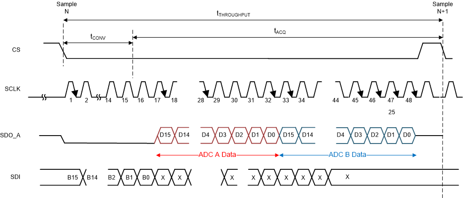
This mode can be selected by writing CFR.B11 = 0 and CFR.B10 = 1. Figure 7-7 shows a detailed timing diagram for this mode.
 Figure 7-7 32-CLK, Single-SDO Mode Timing Diagram
A CS falling edge brings the serial data bus out of 3-state and also outputs a 0 on the SDO_A pin. The device converts the sampled analog input during the conversion time (tCONV). SDO_A reads 0 during this period. After competing the conversion process, the sample-and-hold circuit goes back into sample mode. The device outputs the MSB of ADC_A on the SDO_A pin on the 16th SCLK falling edge. As shown in Table 7-10, the subsequent SCLK falling edges are used to shift out the conversion result of ADC_A followed by the conversion result of ADC_B on the SDO_A pin.
| DEVICE | PIN | LAUNCH EDGE | |||||||||||||||||||
|---|---|---|---|---|---|---|---|---|---|---|---|---|---|---|---|---|---|---|---|---|---|
| CS | SCLK | CS | |||||||||||||||||||
| ↓ | ↓1 | — | ↓15 | ↓16 | — | ↓27 | ↓28 | ↓29 | ↓30 | ↓31 | ↓32 | — | ↓43 | ↓44 | ↓45 | ↓46 | ↓47 | ↓48 ... | ↑ | ||
| ADS8353-Q1 | SDO-A | 0 | 0 | — | 0 | D15_A | — | D4_A | D3_A | D2_A | D1_A | D0_A | D15_B | — | D4_B | D3_B | D2_B | D1_B | D0_B | 0 ... | Hi-Z |
In this mode, at least 48 SCLK falling edges must be given to validate the read or write frame. A CS rising edge ends the frame and puts the serial bus into 3-state.
See the Section 6.6 table for timing specifications specific to this serial interface mode.