JAJSGS3B January   2019  – July 2022 ADS8353-Q1

PRODUCTION DATA  

  1. 1特長
  2. 2アプリケーション
  3. 3概要
  4. 4Revision History
  5. 5Pin Configuration and Functions
  6. 6Specifications
    1. 6.1 Absolute Maximum Ratings
    2. 6.2 ESD Ratings
    3. 6.3 Thermal Information
    4. 6.4 Recommended Operating Conditions
    5. 6.5 Electrical Characteristics
    6. 6.6 Timing Requirements
    7. 6.7 Switching Characteristics
    8. 6.8 Timing Diagram
    9. 6.9 Typical Characteristics
  7. 7Detailed Description
    1. 7.1 Overview
    2. 7.2 Functional Block Diagram
    3. 7.3 Feature Description
      1. 7.3.1 Reference
      2. 7.3.2 Analog Inputs
        1. 7.3.2.1 Analog Input: Full-Scale Range Selection
        2. 7.3.2.2 Analog Input: Single-Ended and Pseudo-Differential Configurations
      3. 7.3.3 Transfer Function
    4. 7.4 Device Functional Modes
    5. 7.5 Programming
      1. 7.5.1 Serial Interface
      2. 7.5.2 Write to User-Programmable Registers
      3. 7.5.3 Data Read Operation
        1. 7.5.3.1 Reading User-Programmable Registers
        2. 7.5.3.2 Conversion Data Read
          1. 7.5.3.2.1 32-CLK, Dual-SDO Mode (CFR.B11 = 0, CFR.B10 = 0, Default)
          2. 7.5.3.2.2 32-CLK, Single-SDO Mode (CFR.B11 = 0, CFR.B10 = 1)
      4. 7.5.4 Low-Power Modes
        1. 7.5.4.1 STANDBY Mode
        2. 7.5.4.2 Software Power-Down (SPD) Mode
      5. 7.5.5 Frame Abort, Reconversion, or Short-Cycling
    6. 7.6 Register Maps
      1. 7.6.1 ADS8353-Q1 Registers
  8. 8Application and Implementation
    1. 8.1 Application Information
      1. 8.1.1 Input Amplifier Selection
      2. 8.1.2 Charge Kickback Filter
    2. 8.2 Typical Application
      1. 8.2.1 Design Requirements
      2. 8.2.2 Detailed Design Procedure
      3. 8.2.3 Application Curve
    3. 8.3 Power Supply Recommendations
    4. 8.4 Layout
      1. 8.4.1 Layout Guidelines
      2. 8.4.2 Layout Example
  9. 9Device and Documentation Support
    1. 9.1 Device Support
      1. 9.1.1 Development Support
    2. 9.2 Documentation Support
      1. 9.2.1 Related Documentation
    3. 9.3 Receiving Notification of Documentation Updates
    4. 9.4 サポート・リソース
    5. 9.5 Trademarks
    6. 9.6 Electrostatic Discharge Caution
    7. 9.7 Glossary
      1.      Mechanical, Packaging, and Orderable Information

Analog Inputs

The ADS8353-Q1 supports single-ended or pseudo-differential analog inputs on both ADC channels. These inputs are sampled and converted simultaneously by the two ADCs, ADC_A and ADC_B. ADC_A samples and converts (VAINP_A – VAINM_A), and ADC_B samples and converts (VAINP_B – VAINM_B).

Figure 7-2a and Figure 7-2b show equivalent circuits for the ADC_A and ADC_B analog input pins, respectively. Series resistance, RS, represents the on-state sampling switch resistance (typically 50 Ω) and CSAMPLE is the device sampling capacitor (typically 40 pF).
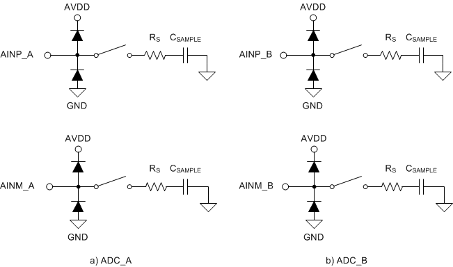
GUID-5B080EB1-688A-41C3-BF81-F588F7F89FE3-low.gifFigure 7-2 Equivalent Circuit for the Analog Input Pins