JAJSH85B April   2019  – April 2019 TPS566235

PRODUCTION DATA.  

  1. 特長
  2. アプリケーション
  3. 概要
    1.     Device Images
      1.      代表的なアプリケーション
      2.      効率と出力電流との関係、Eco-mode
  4. 改訂履歴
  5. Pin Configuration and Functions
    1.     Pin Functions
  6. Specifications
    1. 6.1 Absolute Maximum Ratings
    2. 6.2 ESD Ratings
    3. 6.3 Recommended Operating Conditions
    4. 6.4 Thermal Information
    5. 6.5 Electrical Characteristics
    6. 6.6 Typical Characteristics
  7. Detailed Description
    1. 7.1 Overview
    2. 7.2 Functional Block Diagram
    3. 7.3 Feature Description
      1. 7.3.1 PWM Operation and D-CAP3 Control
      2. 7.3.2 Power Good
      3. 7.3.3 Soft Start and Pre-Biased Soft Start
      4. 7.3.4 Over current Protection and Undervoltage Protection
      5. 7.3.5 Over Voltage Protection
      6. 7.3.6 UVLO Protection
      7. 7.3.7 Thermal Shutdown
    4. 7.4 Device Functional Modes
      1. 7.4.1 Light Load Operation
      2. 7.4.2 MODE Pin Configuration
      3. 7.4.3 Advanced Eco-Mode Control
      4. 7.4.4 Out-Of-Audio Mode
      5. 7.4.5 Force CCM Mode
      6. 7.4.6 Standby Operation
  8. Application and Implementation
    1. 8.1 Application Information
    2. 8.2 Typical Application
      1. 8.2.1 Design Requirements
      2. 8.2.2 Detailed Design Procedure
        1. 8.2.2.1 Custom Design With WEBENCH® Tools
        2. 8.2.2.2 Inductor Selection
        3. 8.2.2.3 Output Capacitor Selection
        4. 8.2.2.4 Input Capacitor Selection
      3. 8.2.3 Application Curves
  9. Power Supply Recommendations
  10. 10Layout
    1. 10.1 Layout Guidelines
    2. 10.2 Layout Example
  11. 11デバイスおよびドキュメントのサポート
    1. 11.1 デバイス・サポート
      1. 11.1.1 デベロッパー・ネットワークの製品に関する免責事項
      2. 11.1.2 開発サポート
        1. 11.1.2.1 WEBENCH®ツールによるカスタム設計
    2. 11.2 ドキュメントの更新通知を受け取る方法
    3. 11.3 コミュニティ・リソース
    4. 11.4 商標
    5. 11.5 静電気放電に関する注意事項
    6. 11.6 Glossary
  12. 12メカニカル、パッケージ、および注文情報

Application Curves

Figure 20 through Figure 35 applies to the circuit of Figure 19. VIN = 12 V, TJ = 25°C (unless otherwise specified)

TPS566235 D001-EfficiencyPSM.gif
Figure 20. Efficiency Curve
TPS566235 D022-FswPSMvsVIN.gif
IOUT = 6 A
Figure 22. Switching Frequency vs Input Voltage
TPS566235 D020-Lineregulation0.gif
Figure 24. Line Regulation, IOUT = 0.1 A
TPS566235 fbd-06-slvsew1.gif
Figure 26. Start-Up Through EN, IOUT = 3 A
TPS566235 fbd-08-slvsew1.gif
Figure 28. Start Up Relative to VIN Rising, IOUT = 3 A
TPS566235 fbd-04-slvsew1.gif
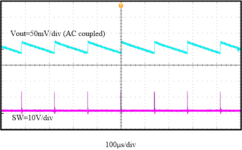
Figure 30. Output Voltage Ripple, IOUT = 0.01 A
TPS566235 fbd-10-slvsew1.gif
Slew Rate=2.5A/µs
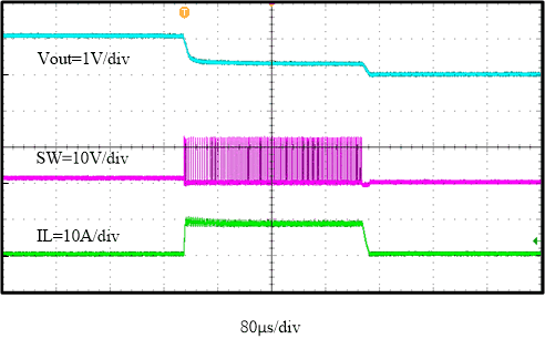
Figure 32. Transient Response, 0.6 A to 5.4 A
TPS566235 fbd-12-slvsew1.gif
Figure 34. Normal Operation to Output Hard Short
TPS566235 D019-LoadregulationPSM.gif
Figure 21. Load Regulation
TPS566235 D016-FswPSM.gif
Figure 23. Switching Frequency vs Output Load
TPS566235 D021-Lineregulation6.gif
Figure 25. Line Regulation, IOUT = 6 A
TPS566235 fbd-07-slvsew1.gif
Figure 27. Shut-down Through EN, IOUT = 3 A
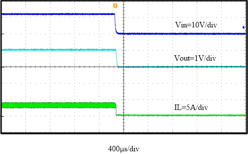
TPS566235 fbd-09-slvsew1.gif
Figure 29. Start Up Relative to VIN Falling, IOUT = 3 A
TPS566235 fbd-05-slvsew1.gif
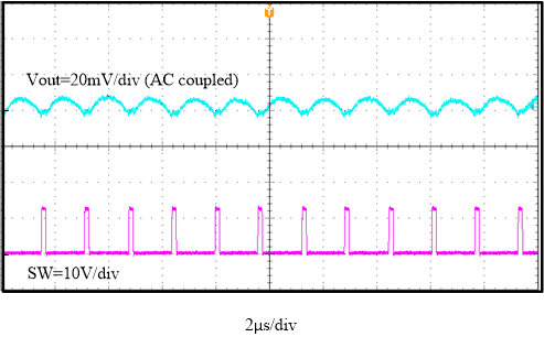
Figure 31. Output Voltage Ripple, IOUT = 6 A
TPS566235 fbd-11-slvsew1.gif
Slew Rate=2.5A/µs
Figure 33. Transient Response, 0 A to 6 A
TPS566235 fbd-13-slvsew1.gif
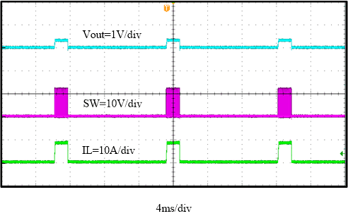
Figure 35. Output Hard Short Hiccup