JAJSHL1J August   2018  – May 2021 TLV803E , TLV809E , TLV810E

PRODMIX  

  1. 特長
  2. アプリケーション
  3. 概要
  4. Revision History
  5. Device Comparison
  6. Pin Configuration and Functions
  7. Specifications
    1. 7.1 Absolute Maximum Ratings
    2. 7.2 ESD Ratings
    3. 7.3 Recommended Operating Conditions
    4. 7.4 Thermal Information
    5. 7.5 Electrical Characteristics
    6. 7.6 Timing Requirements
    7. 7.7 Timing Diagrams
    8. 7.8 Typical Characteristics
  8. Detailed Description
    1. 8.1 Overview
    2. 8.2 Functional Block Diagram
    3. 8.3 Feature Description
      1. 8.3.1 Input Voltage (VDD)
      2. 8.3.2 VDD Hysteresis
      3. 8.3.3 VDD Glitch Immunity
      4. 8.3.4 Manual Reset (MR) Input for X2SON (DPW) Package Only
      5. 8.3.5 Output Logic
        1. 8.3.5.1 RESET Output, Active-Low
        2. 8.3.5.2 RESET Output, Active-High
    4. 8.4 Device Functional Modes
      1. 8.4.1 Normal Operation (VDD > VDD(min))
      2. 8.4.2 VDD Between VPOR and VDD(min)
      3. 8.4.3 Below Power-On-Reset (VDD < VPOR)
  9. Application and Implementation
    1. 9.1 Application Information
    2. 9.2 Typical Application - Voltage Rail Monitoring
      1. 9.2.1 Design Requirements
      2. 9.2.2 Detailed Design Procedure
      3. 9.2.3 Application Curves
    3. 9.3 Typical Application - Overvoltage Monitoring
      1. 9.3.1 Design Requirements
      2. 9.3.2 Detailed Design Procedure
  10. 10Power Supply Recommendations
  11. 11Layout
    1. 11.1 Layout Guidelines
    2. 11.2 Layout Example
  12. 12Device and Documentation Support
    1. 12.1 Device Support
      1. 12.1.1 Device Nomenclature
    2. 12.2 Documentation Support
      1. 12.2.1 Related Documentation
    3. 12.3 Receiving Notification of Documentation Updates
    4. 12.4 サポート・リソース
    5. 12.5 Trademarks
    6. 12.6 Electrostatic Discharge Caution
    7. 12.7 Glossary
  13. 13Mechanical, Packaging, and Orderable Information

Typical Application - Overvoltage Monitoring

A typical use case for the push-pull active-high device variant TLV810E is overvoltage monitoring. The TLV810E can monitor a power supply, a MCU power rail, or a battery during charging for example. The VDD pin monitors the voltage rail and once VDD rises above VIT+, the RESET output deactivates to logic low after the reset delay time tD. If VDD falls below VIT-, the RESET output activates to logic high after the propagation delay (tPD_HL). The voiltage thresholds and the reset delay time depends on the device variant. See Section 5 for device variant naming nomenclature.
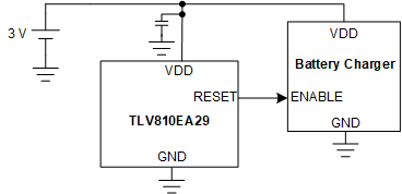
GUID-20200927-CA0I-RKJB-STG3-LJMK3VWJHZXQ-low.gif Figure 9-4 TLV810E Overvoltage Monitor Circuit for Battery Charger