JAJSHR4B August   2019  – April 2020 AMC1336

PRODUCTION DATA.  

  1. 特長
  2. アプリケーション
  3. 概要
    1.     Device Images
      1.      概略回路図
  4. 改訂履歴
  5. Pin Configuration and Functions
    1.     Pin Functions
  6. Specifications
    1. Table 1.  Absolute Maximum Ratings
    2. Table 2.  ESD Ratings
    3. Table 3.  Recommended Operating Conditions
    4. Table 4.  Thermal Information
    5. Table 5.  Power Ratings
    6. Table 6.  Insulation Specifications
    7. Table 7.  Safety-Related Certifications
    8. Table 8.  Safety Limiting Values
    9. Table 9.  Electrical Characteristics
    10. Table 10. Switching Characteristics
    11. 6.1       Insulation Characteristics Curves
    12. 6.2       Typical Characteristics
  7. Detailed Description
    1. 7.1 Overview
    2. 7.2 Functional Block Diagram
    3. 7.3 Feature Description
      1. 7.3.1 Analog Input
      2. 7.3.2 Modulator
      3. 7.3.3 Isolation Channel Signal Transmission
      4. 7.3.4 Clock Input
      5. 7.3.5 Digital Output
    4. 7.4 Device Functional Modes
      1. 7.4.1 Output Behavior in Case of a Full-Scale Input
      2. 7.4.2 AVDD Diagnostics and Fail-Safe Output
  8. Application and Implementation
    1. 8.1 Application Information
      1. 8.1.1 Digital Filter Usage
    2. 8.2 Typical Application
      1. 8.2.1 Design Requirements
      2. 8.2.2 Detailed Design Procedure
      3. 8.2.3 Application Curve
      4. 8.2.4 What to Do and What Not to Do
  9. Power Supply Recommendations
  10. 10Layout
    1. 10.1 Layout Guidelines
    2. 10.2 Layout Example
  11. 11デバイスおよびドキュメントのサポート
    1. 11.1 デバイス・サポート
      1. 11.1.1 デバイスの項目表記
        1. 11.1.1.1 絶縁の用語集
    2. 11.2 ドキュメントのサポート
      1. 11.2.1 関連資料
    3. 11.3 ドキュメントの更新通知を受け取る方法
    4. 11.4 コミュニティ・リソース
    5. 11.5 商標
    6. 11.6 静電気放電に関する注意事項
    7. 11.7 Glossary
  12. 12メカニカル、パッケージ、および注文情報

Typical Characteristics

at AVDD = 5 V, DVDD = 3.3 V, AINP = –1 V to 1 V, AINN = AGND, fCLKIN = 20 MHz, and sinc3 filter with OSR = 256 (unless otherwise noted)
AMC1336 D003_SBAS951.gif
Figure 6. Input Bias Current vs
Common-Mode Input Voltage
AMC1336 D005_SBAS951.gif
Figure 8. Integral Nonlinearity vs Temperature
AMC1336 D006_SBAS951.gif
Figure 10. Offset Error vs High-Side Supply Voltage
AMC1336 D008_SBAS951.gif
fCLKIN < 9 MHz with AVDD ≥ 4.5 V only
Figure 12. Offset Error vs Clock Frequency
AMC1336 D011_SBAS951.gif
Figure 14. Gain Error vs High-Side Supply Voltage
AMC1336 D013_SBAS951.gif
fCLKIN < 9 MHz with AVDD ≥ 4.5 V only
Figure 16. Gain Error vs Clock Frequency
AMC1336 D010_SBAS951.gif
Figure 18. Power-Supply Rejection Ratio vs
Ripple Frequency
AMC1336 D015_SBAS951.gif
Figure 20. Signal-to-Noise Ratio and Signal-to-Noise + Distortion vs Temperature
AMC1336 D017_SBAS951.gif
Figure 22. Signal-to-Noise Ratio and Signal-to-Noise + Distortion vs Input Signal Frequency
AMC1336 D019_SBAS951.gif
Figure 24. Total Harmonic Distortion vs
High-Side Supply Voltage
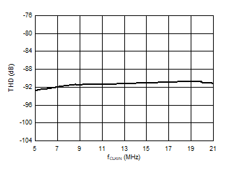
AMC1336 D021_SBAS951.gif
fCLKIN < 9 MHz with AVDD ≥ 4.5 V only
Figure 26. Total Harmonic Distortion vs Clock Frequency
AMC1336 D023_SBAS951.gif
Figure 28. Total Harmonic Distortion vs
Input Signal Amplitude
AMC1336 D025_SBAS951.gif
Figure 30. Spurious-Free Dynamic Range vs Temperature
AMC1336 D027_SBAS951.gif
Figure 32. Spurious-Free Dynamic Range vs
Input Signal Frequency
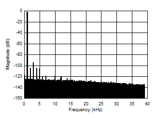
AMC1336 D029_SBAS951.gif
156,250-point DFT, VIN = 2 VPP
Figure 34. Frequency Spectrum with 1-kHz Input Signal
AMC1336 D031_SBAS951.gif
Figure 36. Supply Current vs Supply Voltage
AMC1336 D033_SBAS951.gif
fCLKIN < 9 MHz with AVDD ≥ 4.5 V only
Figure 38. Supply Current vs Clock Frequency
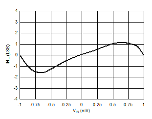
AMC1336 D004_SBAS951.gif
Figure 7. Integral Nonlinearity vs
Input Voltage
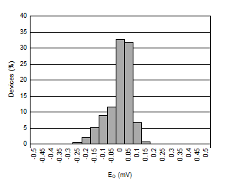
AMC1336 D038_SBAS951.gif
Figure 9. Offset Error Histogram
AMC1336 D007_SBAS951.gif
Figure 11. Offset Error vs Temperature
AMC1336 D039_SBAS951.gif
Figure 13. Gain Error Histogram
AMC1336 D012_SBAS951.gif
Figure 15. Gain Error vs Temperature
AMC1336 D009_SBAS951.gif
Figure 17. Common-Mode Rejection Ratio vs
Input Signal Frequency
AMC1336 D014_SBAS951.gif
Figure 19. Signal-to-Noise Ratio and Signal-to-Noise + Distortion vs High-Side Supply Voltage
AMC1336 D016_SBAS951.gif
fCLKIN < 9 MHz with AVDD ≥ 4.5 V only
Figure 21. Signal-to-Noise Ratio and Signal-to-Noise + Distortion vs Clock Frequency
AMC1336 D018_SBAS951.gif
Figure 23. Signal-to-Noise Ratio and Signal-to-Noise + Distortion vs Input Signal Amplitude
AMC1336 D020_SBAS951.gif
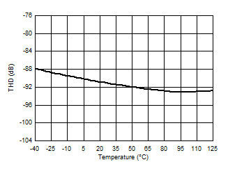
Figure 25. Total Harmonic Distortion vs Temperature
AMC1336 D022_SBAS951.gif
Figure 27. Total Harmonic Distortion vs
Input Signal Frequency
AMC1336 D024_SBAS951.gif
Figure 29. Spurious-Free Dynamic Range vs
High-Side Supply Voltage
AMC1336 D026_SBAS951.gif
fCLKIN < 9 MHz with AVDD ≥ 4.5 V only
Figure 31. Spurious-Free Dynamic Range vs
Clock Frequency
AMC1336 D028_SBAS951.gif
Figure 33. Spurious-Free Dynamic Range vs
Input Signal Amplitude
AMC1336 D030_SBAS951.gif
156,250-point DFT, VIN = 2 VPP
Figure 35. Frequency Spectrum with 10-kHz Input Signal
AMC1336 D032_SBAS951.gif
Figure 37. Supply Current vs Temperature