JAJSHZ5D September 2019 – November 2023 UCC21750-Q1
PRODUCTION DATA
- 1
- 1 特長
- 2 アプリケーション
- 3 概要
- 4 Revision History
- 5 Pin Configuration and Functions
-
6 Specifications
- 6.1 Absolute Maximum Ratings
- 6.2 ESD Ratings
- 6.3 Recommended Operating Conditions
- 6.4 Thermal Information
- 6.5 Power Ratings
- 6.6 Insulation Specifications
- 6.7 Safety Limiting Values
- 6.8 Electrical Characteristics
- 6.9 Safety-Related Certifications
- 6.10 Switching Characteristics
- 6.11 Insulation Characteristics Curves
- 6.12 Typical Characteristics
- 7 Parameter Measurement Information
-
8 Detailed Description
- 8.1 Overview
- 8.2 Functional Block Diagram
- 8.3
Feature Description
- 8.3.1 Power Supply
- 8.3.2 Driver Stage
- 8.3.3 VCC and VDD Undervoltage Lockout (UVLO)
- 8.3.4 Active Pulldown
- 8.3.5 Short Circuit Clamping
- 8.3.6 Internal Active Miller Clamp
- 8.3.7 Desaturation (DESAT) Protection
- 8.3.8 Soft Turn-Off
- 8.3.9 Fault (FLT, Reset, and Enable (RST/EN)
- 8.3.10 Isolated Analog to PWM Signal Function
- 8.4 Device Functional Modes
-
9 Applications and Implementation
- 9.1 Application Information
- 9.2
Typical Application
- 9.2.1 Design Requirements
- 9.2.2
Detailed Design Procedure
- 9.2.2.1 Input Filters for IN+, IN–, and RST/EN
- 9.2.2.2 PWM Interlock of IN+ and IN–
- 9.2.2.3 FLT, RDY, and RST/EN Pin Circuitry
- 9.2.2.4 RST/EN Pin Control
- 9.2.2.5 Turn-On and Turn-Off Gate Resistors
- 9.2.2.6 Overcurrent and Short Circuit Protection
- 9.2.2.7 Isolated Analog Signal Sensing
- 9.2.2.8 Higher Output Current Using an External Current Buffer
- 9.2.3 Application Curves
- 10Power Supply Recommendations
- 11Layout
- 12Device and Documentation Support
- 13Mechanical, Packaging, and Orderable Information
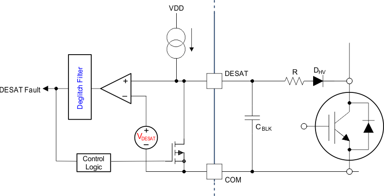
8.3.7 Desaturation (DESAT) Protection
The UCC21750-Q1 implements a fast overcurrent and short circuit protection feature to protect the IGBT module from catastrophic breakdown during fault. The DESAT pin of the device has a typical 9-V threshold with respect to COM, source or emitter of the power semiconductor. When the input is in floating condition, or the output is held in low state, the DESAT pin is pulled down by an internal MOSFET and held in LOW state, which prevents the overcurrent and short circuit fault from false triggering. The internal current source of the DESAT pin is activated only during the driver ON state, which means the overcurrent and short circuit protection feature only works when the power semiconductor is in on state. The internal pulldown MOSFET helps to discharge the voltage of DESAT pin when the power semiconductor is turned off. The UCC21750-Q1 features a 200-ns internal leading edge blanking time after the OUTH switches to high state. The internal current source is activated to charge the external blanking capacitor after the internal leading edge blanking time. The typical value of the internal current source is 500 µA.
 Figure 8-5 DESAT Protection