JAJSI70C
May 2008 – November 2019
DAC9881
PRODUCTION DATA.
1
特長
2
アプリケーション
3
概要
Device Images
ブロック図
4
改訂履歴
5
概要(続き)
6
Pin Configuration and Functions
Pin Functions
7
Specifications
7.1
Absolute Maximum Ratings
7.2
ESD Ratings
7.3
Recommended Operating Conditions
7.4
Thermal Information
7.5
Electrical Characteristics: AVDD = 5 V
7.6
Electrical Characteristics: AVDD = 2.7 V
7.7
Timing Requirements—Standalone Operation Without SDO
7.8
Timing Requirements—Standalone Operation With SDO and Daisy-Chain Mode
7.9
Typical Characteristics: AVDD = 5 V
7.10
Typical Characteristics: AVDD = 2.7 V
8
Detailed Description
8.1
Overview
8.2
Functional Block Diagram
8.3
Feature Description
8.3.1
Analog Output
8.3.2
Reference Inputs
8.3.3
Output Range
8.3.4
Input Data Format
8.3.5
Hardware Reset
8.3.6
Power-On Reset
8.3.6.1
Program Reset Value
8.3.7
Power Down
8.3.8
Double-Buffered Interface
8.3.8.1
Load DAC Pin (LDAC)
8.3.8.1.1
Synchronous Mode
8.3.8.1.2
Asynchronous Mode
8.3.9
1.8-V to 5-V Logic Interface
8.3.10
Power-Supply Sequence
8.4
Device Functional Modes
8.4.1
Serial Interface
8.4.1.1
Input Shift Register
8.4.1.1.1
Stand-Alone Mode
8.4.1.1.2
Daisy-Chain Mode
9
Application and Implementation
9.1
Application Information
9.1.1
Bipolar Operation Using the DAC9881
9.2
Typical Application
9.2.1
DAC9881 Sample-and-Hold Circuit
9.2.1.1
Design Requirements
9.2.1.2
Detailed Design Procedure
9.2.1.3
Application Curves
9.3
System Example
10
Power Supply Recommendations
11
Layout
11.1
Layout Guidelines
11.2
Layout Example
12
デバイスおよびドキュメントのサポート
12.1
ドキュメントのサポート
12.1.1
関連資料
12.2
ドキュメントの更新通知を受け取る方法
12.3
サポート・リソース
12.4
商標
12.5
静電気放電に関する注意事項
12.6
Glossary
13
メカニカル、パッケージ、および注文情報
7.9
Typical Characteristics: AV
DD
= 5 V
at T
A
= 25°C, V
REFH
= 5 V, V
REFL
= 0 V, and gain = 1X mode (unless otherwise noted)
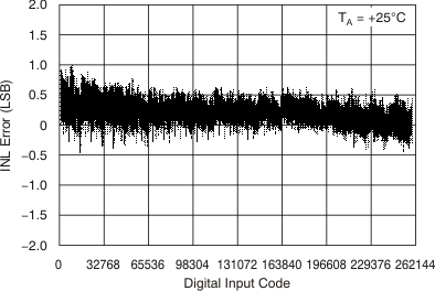
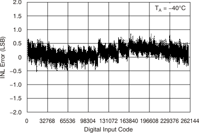
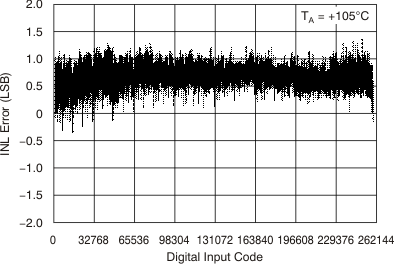
Figure 4.
Linearity Error vs Digital Input Code
Figure 6.
Linearity Error vs Digital Input Code
Figure 8.
Linearity Error vs Digital Input Code
Figure 10.
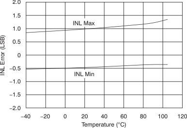
Linearity Error vs Temperature
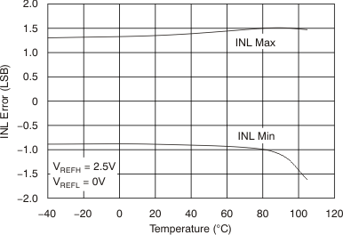
Gain = 2X mode
Figure 12.
Linearity Error vs Temperature
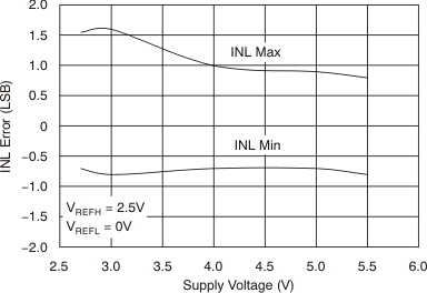
Figure 14.
Linearity Error vs Supply Voltage
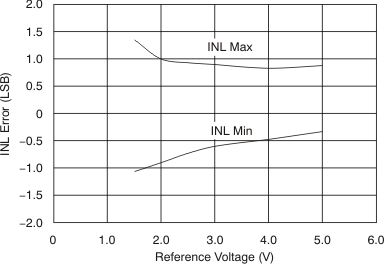
Figure 16.
Linearity Error vs Reference Voltage
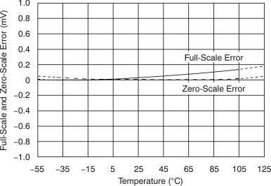
Figure 18.
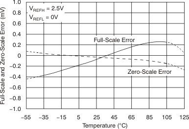
Full-Scale and Zero-Scale Error vs Temperature
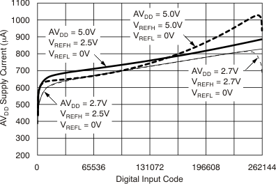
Figure 20.
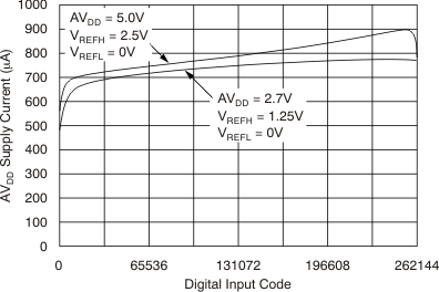
AVDD Supply Current vs Digital Input Code
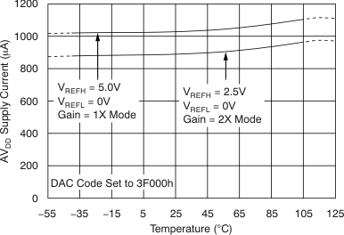
Figure 22.
AVDD Supply Current vs Temperature
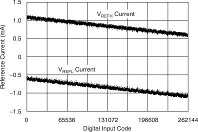
Figure 24.
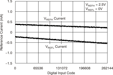
Reference Current vs Digital Input Code
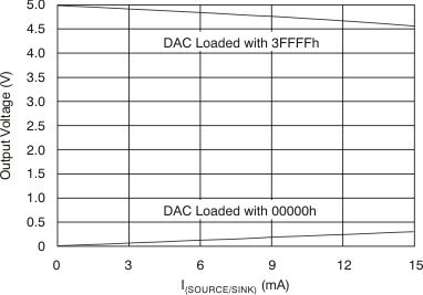
Figure 26.
Output Voltage vs Drive Current Capability
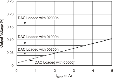
Figure 28.
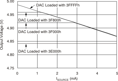
Output Voltage vs Drive Current Capability (Operation Near AGND Rail)
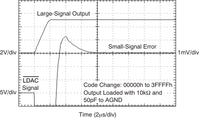
Figure 30.
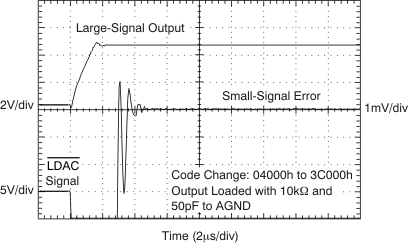
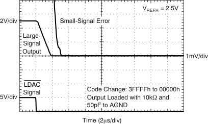
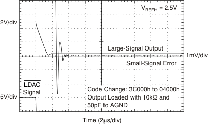
Large-Signal Settling Time
Figure 32.
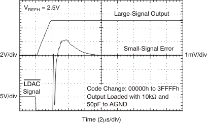
Large-Signal Settling Time
Gain = 2X mode
Figure 34.
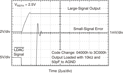
Large-Signal Settling Time
Gain = 2X mode
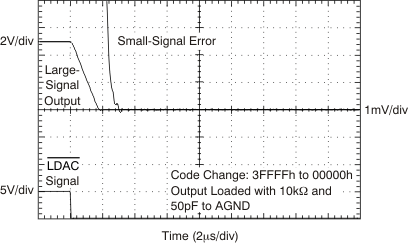
Figure 36.
Large-Signal Settling Time
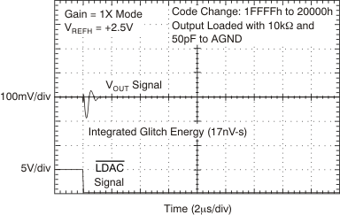
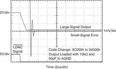
Figure 38.
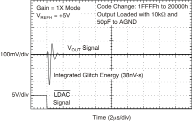
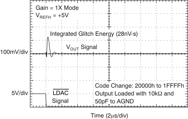
Major Carry Glitch
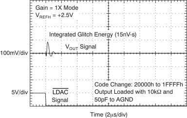
Figure 40.
Major Carry Glitch
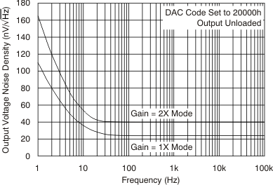
Figure 42.
Output Noise Density vs Frequency
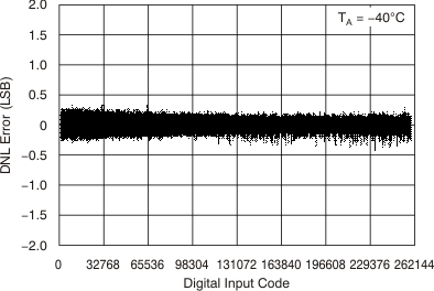
Figure 5.
Differential Linearity Error vs Digital Input Code
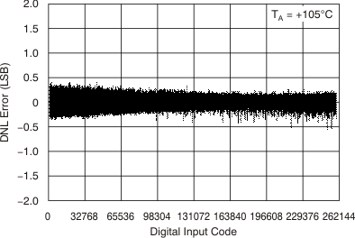
Figure 7.
Differential Linearity Error vs Digital Input Code
Figure 9.
Differential Lineary Error vs Digital Input Code
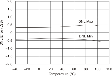
Figure 11.
Differential Linearity Error vs Temperature
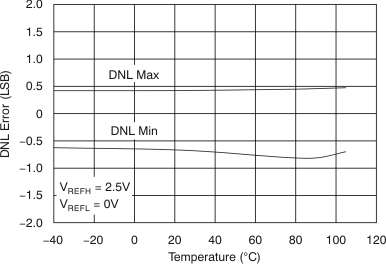
Gain = 2X mode
Figure 13.
Differential Linearity Error vs Temperature
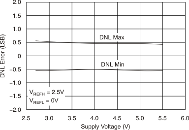
Figure 15.
Differential Linearity Error vs Supply Voltage
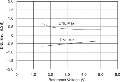
Figure 17.
Differential Linearity Error vs Reference Voltage
Gain = 2X mode
Figure 19.
Full-Scale and Zero-Scale Error vs Temperature
Gain = 2X mode
Figure 21.
AVDD Supply Current vs Digital Input Code
Figure 23.
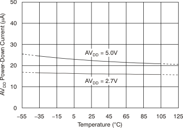
AVDD Power-Down Current vs Temperature
Gain = 2X mode
Figure 25.
Reference Current vs Digital Input Code
Figure 27.
Output Voltage vs Drive Current Capability (Operation Near AV
DD
Rail)
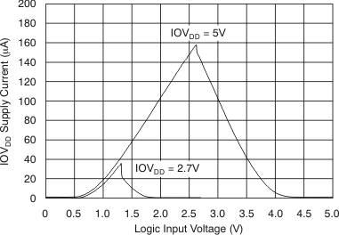
Figure 29.
IOVDD Supply Current vs Logic Input Voltage
Figure 31.
Large-Signal Settling Time
Figure 33.
Large-Signal Settling Time
Gain = 2X mode
Figure 35.
Large-Signal Settling Time
Gain = 2X mode
Figure 37.
Large-Signal Settling Time
Figure 39.
Major Carry Glitch
Figure 41.
Major Carry Glitch
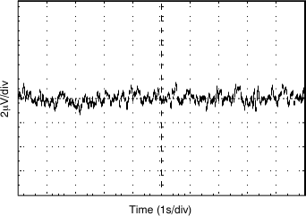
Figure 43.
Low-Frequency Output Noise (0.1 Hz to 10 Hz)