JAJSI70C May 2008 – November 2019 DAC9881
PRODUCTION DATA.
- 1 特長
- 2 アプリケーション
- 3 概要
- 4 改訂履歴
- 5 概要(続き)
- 6 Pin Configuration and Functions
-
7 Specifications
- 7.1 Absolute Maximum Ratings
- 7.2 ESD Ratings
- 7.3 Recommended Operating Conditions
- 7.4 Thermal Information
- 7.5 Electrical Characteristics: AVDD = 5 V
- 7.6 Electrical Characteristics: AVDD = 2.7 V
- 7.7 Timing Requirements—Standalone Operation Without SDO
- 7.8 Timing Requirements—Standalone Operation With SDO and Daisy-Chain Mode
- 7.9 Typical Characteristics: AVDD = 5 V
- 7.10 Typical Characteristics: AVDD = 2.7 V
-
8 Detailed Description
- 8.1 Overview
- 8.2 Functional Block Diagram
- 8.3 Feature Description
- 8.4 Device Functional Modes
- 9 Application and Implementation
- 10Power Supply Recommendations
- 11Layout
- 12デバイスおよびドキュメントのサポート
- 13メカニカル、パッケージ、および注文情報
8.3.1 Analog Output
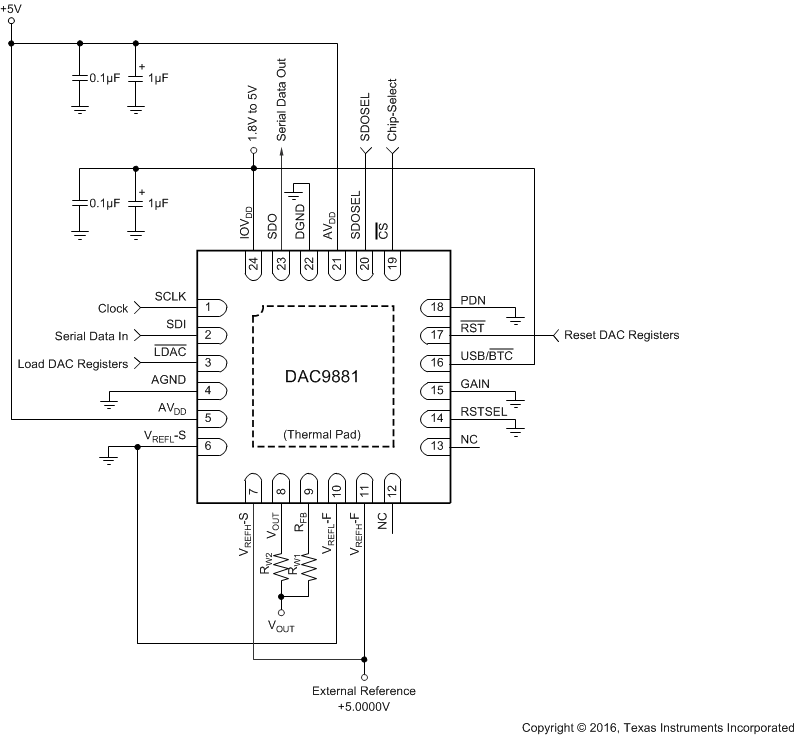
The DAC9881 offers a force and sense output configuration for the high open-loop gain output amplifier. This feature allows the loop around the output amplifier to be closed at the load (as shown in Figure 66), thus ensuring an accurate output voltage. The output buffer VOUT and RFB pins are provided so that the output op amp buffer feedback can be connected at the load. Without a driven load, the DAC9881 output typically swings to within 15 mV of the AGND and AVDD supply rails. Because of the high accuracy of these DACs, system design problems such as grounding and wiring resistance become very important. A 18-bit converter with a 5-V full-scale range has an LSB value of 19 µV. The DAC9881 has a typical feedback resistor current of 0.5 mA; thus, a series wiring resistance of only 100 mΩ (RW1) causes a voltage drop of 50 µV. In terms of a system layout, the resistivity of a typical 1-ounce copper-clad printed circuit board (PCB) is 0.5-mΩ per square. For a 0.5-mA current, a 0.25-mm wide printed-circuit conductor 25-mm long results in a voltage drop of 25 µV.
NOTE
the wiring resistance of RW2 is not critical as long as the feedback resistor (RFB) is connected at the driven load.
 Figure 66. Analog Output Closed-Loop Configuration
(RW1 and RW2 Represent Wiring Resistance)