JAJSIG0A
January 2020 – February 2022
BQ25616
PRODUCTION DATA
1
特長
2
アプリケーション
3
概要
4
Revision History
5
概要 (続き)
6
Device Comparison Table
7
Pin Configuration and Functions
8
Specifications
8.1
Absolute Maximum Ratings
8.2
ESD Ratings
8.3
Recommended Operating Conditions
8.4
Thermal Information
8.5
Electrical Characteristics
8.6
Timing Requirements
8.7
Typical Characteristics
9
Detailed Description
9.1
Overview
9.2
Functional Block Diagram
9.3
Feature Description
9.3.1
Power-On-Reset (POR)
9.3.2
Device Power Up From Battery Without Input Source
9.3.3
Power Up From Input Source
9.3.3.1
Power Up ACFET
9.3.3.2
Power Up REGN LDO
9.3.3.3
Poor Source Qualification
9.3.3.4
Input Source Type Detection (IINDPM Threshold)
9.3.3.4.1
D+/D– Detection Sets Input Current Limit
9.3.3.5
Input Voltage Limit Threshold Setting (VINDPM Threshold)
9.3.3.6
Power Up Converter in Buck Mode
9.3.4
Boost Mode Operation From Battery
9.3.5
Standalone Charger
9.3.6
Power Path Management
9.3.6.1
Narrow VDC Architecture
9.3.6.2
Dynamic Power Management
9.3.6.3
Supplement Mode
9.3.7
Battery Charging Management
9.3.7.1
Autonomous Charging Cycle
9.3.7.2
Battery Charging Profile
9.3.7.3
Charging Termination
9.3.7.4
Thermistor Qualification
9.3.7.4.1
JEITA Guideline Compliance During Charging Mode (BQ25616J)
9.3.7.4.2
Hot/Cold Temperature Window During Charging Mode (BQ25616)
9.3.7.4.3
Boost Mode Thermistor Monitor During Battery Discharge Mode
9.3.7.5
Charging Safety Timer
9.3.8
Status Outputs ( PG, STAT)
9.3.8.1
Power Good Indicator ( PG Pin )
9.3.8.2
Charging Status Indicator (STAT)
9.3.9
Protections
9.3.9.1
Input Current Limit
9.3.9.2
Voltage and Current Monitoring in Buck Mode
9.3.9.2.1
Input Overvoltage Protection (ACOV)
9.3.9.2.2
System Overvoltage Protection (SYSOVP)
9.3.9.3
Voltage and Current Monitoring in Boost Mode
9.3.9.3.1
Boost Mode Overvoltage Protection
9.3.9.4
Thermal Regulation and Thermal Shutdown
9.3.9.4.1
Thermal Protection in Buck Mode
9.3.9.4.2
Thermal Protection in Boost Mode
9.3.9.5
Battery Protection
9.3.9.5.1
Battery Overvoltage Protection (BATOVP)
9.3.9.5.2
Battery Overdischarge Protection
9.3.9.5.3
System Overcurrent Protection
9.4
Device Functional Modes
10
Application and Implementation
10.1
Application Information
10.2
Typical Applications
10.2.1
BQ25616/616J Application without External OVP
10.2.1.1
Design Requirements
10.2.1.2
Detailed Design Procedure
10.2.1.2.1
Inductor Selection
10.2.1.2.2
Input Capacitor and Resistor
10.2.1.2.3
Output Capacitor
10.2.1.3
Application Curves
10.2.2
BQ25616/616J Application with External OVP
10.2.2.1
Design Requirements
10.2.2.2
Detailed Design Procedure
10.2.2.3
Application Curves
11
Power Supply Recommendations
12
Layout
12.1
Layout Guidelines
12.2
Layout Example
13
Device and Documentation Support
13.1
Device Support
13.1.1
Third-Party Products Disclaimer
13.2
Documentation Support
13.2.1
Related Documentation
13.3
Receiving Notification of Documentation Updates
13.4
サポート・リソース
13.5
Trademarks
13.6
Electrostatic Discharge Caution
13.7
Glossary
14
Mechanical, Packaging, and Orderable Information
12.2
Layout Example
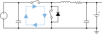
Figure 12-1
High Frequency Current Path
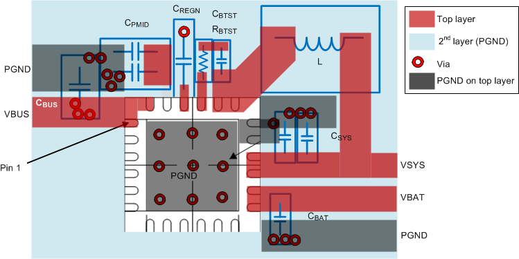
Figure 12-2
Layout Example