JAJSIK5D February 2020 – February 2024 AWR2243
PRODUCTION DATA
- 1
- 1 特長
- 2 アプリケーション
- 3 概要
- 4 機能ブロック図
- 5 Device Comparison
- 6 Terminal Configuration and Functions
-
7 Specifications
- 7.1 Absolute Maximum Ratings
- 7.2 ESD Ratings
- 7.3 Power-On Hours (POH)
- 7.4 Recommended Operating Conditions
- 7.5 Power Supply Specifications
- 7.6 Power Consumption Summary
- 7.7 RF Specification
- 7.8 Thermal Resistance Characteristics for FCBGA Package [ABL0161]
- 7.9
Timing and Switching Characteristics
- 7.9.1 Power Supply Sequencing and Reset Timing
- 7.9.2 Synchronized Frame Triggering
- 7.9.3 Input Clocks and Oscillators
- 7.9.4 Multibuffered / Standard Serial Peripheral Interface (MibSPI)
- 7.9.5 Inter-Integrated Circuit Interface (I2C)
- 7.9.6 LVDS Interface Configuration
- 7.9.7 General-Purpose Input/Output
- 7.9.8 Camera Serial Interface (CSI)
- 8 Detailed Description
- 9 Monitoring and Diagnostic Mechanisms
- 10Applications, Implementation, and Layout
- 11Device and Documentation Support
- 12Revision History
- 13Mechanical, Packaging, and Orderable Information
8.3.1.2 Transmit Subsystem
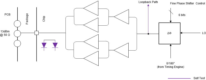
The AWR2243 transmit subsystem consists of three parallel transmit chains, each with independent phase and amplitude control. All three transmitters can be used simultaneously or in time-multiplexed fashion. The device supports binary phase modulation for MIMO radar and interference mitigation. For AWR2243, additional phase shifters are associated with Tx channels, and these can programmed on a per chirp basis.
Each transmit chain can deliver a maximum of 13 dBm at the antenna port on the PCB. The transmit chains also support programmable backoff for system optimization.
Figure 8-2 describes the transmit subsystem.
 Figure 8-2 Transmit Subsystem (Per Channel)