JAJSIK5D February 2020 – February 2024 AWR2243
PRODUCTION DATA
- 1
- 1 特長
- 2 アプリケーション
- 3 概要
- 4 機能ブロック図
- 5 Device Comparison
- 6 Terminal Configuration and Functions
-
7 Specifications
- 7.1 Absolute Maximum Ratings
- 7.2 ESD Ratings
- 7.3 Power-On Hours (POH)
- 7.4 Recommended Operating Conditions
- 7.5 Power Supply Specifications
- 7.6 Power Consumption Summary
- 7.7 RF Specification
- 7.8 Thermal Resistance Characteristics for FCBGA Package [ABL0161]
- 7.9
Timing and Switching Characteristics
- 7.9.1 Power Supply Sequencing and Reset Timing
- 7.9.2 Synchronized Frame Triggering
- 7.9.3 Input Clocks and Oscillators
- 7.9.4 Multibuffered / Standard Serial Peripheral Interface (MibSPI)
- 7.9.5 Inter-Integrated Circuit Interface (I2C)
- 7.9.6 LVDS Interface Configuration
- 7.9.7 General-Purpose Input/Output
- 7.9.8 Camera Serial Interface (CSI)
- 8 Detailed Description
- 9 Monitoring and Diagnostic Mechanisms
- 10Applications, Implementation, and Layout
- 11Device and Documentation Support
- 12Revision History
- 13Mechanical, Packaging, and Orderable Information
8.3.1.1 Clock Subsystem
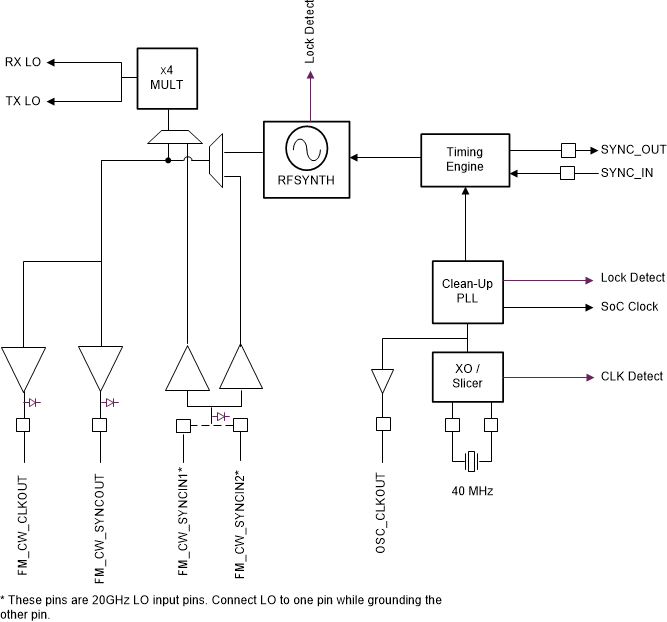
The AWR2243 clock subsystem generates 76 to 81 GHz from an input reference of 40-MHz crystal. It has a built-in oscillator circuit followed by a clean-up PLL and a RF synthesizer circuit. The output of the RF synthesizer is then processed by an X4 multiplier to create the required frequency in the 76 to 81 GHz spectrum. The RF synthesizer output is modulated by the timing engine block to create the required waveforms for effective sensor operation.
The output of the RF synthesizer is available at the device pin boundary for multichip cascaded configuration. The clean-up PLL also provides a reference clock for the host processor after system wakeup.
The clock subsystem also has built-in mechanisms for detecting the presence of a crystal and monitoring the quality of the generated clock.
Figure 8-1 describes the clock subsystem.
 Figure 8-1 Clock
Subsystem