JAJSIL5B February 2020 – October 2024 ADC12DJ1600-Q1 , ADC12QJ1600-Q1 , ADC12SJ1600-Q1
PRODUCTION DATA
- 1
- 1 特長
- 2 アプリケーション
- 3 概要
- 4 Pin Configuration and Functions
-
5 Specifications
- 5.1 Absolute Maximum Ratings
- 5.2 ESD Ratings
- 5.3 Recommended Operating Conditions
- 5.4 Thermal Information
- 5.5 Electrical Characteristics: DC Specifications
- 5.6 ADC12xJ1600-Q1: Electrical Characteristics: Power Consumption
- 5.7 ADC12xJ1600-Q1: Electrical Characteristics: AC Specifications
- 5.8 Timing Requirements
- 5.9 Switching Characteristics
- 5.10 Typical Characteristics
-
6 Detailed Description
- 6.1 Overview
- 6.2 Functional Block Diagram
- 6.3
Feature Description
- 6.3.1 Device Comparison
- 6.3.2 Analog Input
- 6.3.3 Temperature Monitoring Diode
- 6.3.4 Timestamp
- 6.3.5 Clocking
- 6.3.6
JESD204C Interface
- 6.3.6.1 Transport Layer
- 6.3.6.2 Scrambler
- 6.3.6.3 Link Layer
- 6.3.6.4 8B/10B Link Layer
- 6.3.6.5 64B/66B Link Layer
- 6.3.6.6 Physical Layer
- 6.3.6.7 JESD204C Enable
- 6.3.6.8 Multi-Device Synchronization and Deterministic Latency
- 6.3.6.9 Operation in Subclass 0 Systems
- 6.3.6.10 Alarm Monitoring
- 6.4
Device Functional Modes
- 6.4.1 Low Power Mode and High Performance Mode
- 6.4.2 JESD204C Modes
- 6.4.3 Power-Down Modes
- 6.4.4 Test Modes
- 6.4.5 Calibration Modes and Trimming
- 6.4.6 Offset Calibration
- 6.4.7 Trimming
- 6.5 Programming
- 7 Application and Implementation
- 8 Device and Documentation Support
- 9 Revision History
- 10Mechanical, Packaging, and Orderable Information
6.3.2 Analog Input
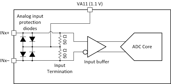
The analog input of the device has an internal buffer to enable high input bandwidth and to isolate sampling capacitor glitch noise from the input circuit. The analog input must be driven differentially because operation with a single-ended signal results in degraded performance. Both AC-coupling and DC-coupling of the analog input is supported. The analog input is designed for an input common-mode voltage (VCMI) of 1.1 V, which is terminated internally through single-ended, 50-Ω resistors to the VA11 supply on each input pin. DC-coupled input signals must have a common-mode voltage that meets the device input common-mode requirements specified as VCMI in the Recommended Operating Conditions table. The device includes internal analog input protection to protect the ADC input during over-range input conditions; see the Analog Input Protection section. Figure 6-4 provides a simplified analog input model.
 Figure 6-4 Analog Input Internal Termination and Protection Diagram