JAJSIY6C December   2011  – April 2020 ADS1291 , ADS1292 , ADS1292R

PRODUCTION DATA.  

  1. 特長
  2. アプリケーション
    1.     ブロック概略図
  3. 概要
  4. 改訂履歴
  5. Pin Configuration and Functions
    1.     Pin Functions
  6. Specifications
    1. 6.1 Absolute Maximum Ratings
    2. 6.2 ESD Ratings
    3. 6.3 Recommended Operating Conditions
    4. 6.4 Thermal Information
    5. 6.5 Electrical Characteristics
    6. 6.6 Timing Requirements
    7. 6.7 Typical Characteristics
  7. Parameter Measurement Information
    1. 7.1 Noise Measurements
  8. Detailed Description
    1. 8.1 Overview
    2. 8.2 Functional Block Diagram
    3. 8.3 Feature Description
      1. 8.3.1  EMI Filter
      2. 8.3.2  Input Multiplexer
        1. 8.3.2.1 Device Noise Measurements
        2. 8.3.2.2 Test Signals (TestP and TestN)
        3. 8.3.2.3 Auxiliary Differential Input (RESP_MODN/IN3N, RESP_MODN/IN3P)
        4. 8.3.2.4 Temperature Sensor (TEMPP, TEMPN)
        5. 8.3.2.5 Supply Measurements (MVDDP, MVDDN)
        6. 8.3.2.6 Lead-Off Excitation Signals (LoffP, LoffN)
        7. 8.3.2.7 Auxiliary Single-Ended Input
      3. 8.3.3  Analog Input
      4. 8.3.4  PGA Settings and Input Range
        1. 8.3.4.1 Input Common-Mode Range
        2. 8.3.4.2 Input Differential Dynamic Range
        3. 8.3.4.3 ADC ΔΣ Modulator
      5. 8.3.5  Digital Decimation Filter
        1. 8.3.5.1 Sinc Filter Stage (sinx / x)
      6. 8.3.6  Reference
      7. 8.3.7  Clock
      8. 8.3.8  Data Format
      9. 8.3.9  Multiple Device Configuration
        1. 8.3.9.1 Standard Mode
      10. 8.3.10 ECG-Specific Functions
        1. 8.3.10.1 Input Multiplexer (Rerouting the Right Leg Drive Signal)
          1. 8.3.10.1.1 Input Multiplexer (Measuring the Right Leg Drive Signal)
        2. 8.3.10.2 Lead-Off Detection
          1. 8.3.10.2.1 DC Lead-Off
          2. 8.3.10.2.2 AC Lead-Off
          3. 8.3.10.2.3 RLD Lead-Off
          4. 8.3.10.2.4 Right Leg Drive (RLD DC Bias Circuit)
            1. 8.3.10.2.4.1 RLD Configuration With Multiple Devices
        3. 8.3.10.3 PACE Detect
        4. 8.3.10.4 Respiration
          1. 8.3.10.4.1 Internal Respiration Circuitry With Internal Clock (ADS1292R)
          2. 8.3.10.4.2 Internal Respiration Circuitry With External Clock (ADS1292R)
      11. 8.3.11 Setting the Device for Basic Data Capture
        1. 8.3.11.1 Lead-Off
    4. 8.4 Device Functional Modes
    5. 8.5 Programming
      1. 8.5.1 SPI Interface
        1. 8.5.1.1  Chip Select (CS)
        2. 8.5.1.2  Serial Clock (SCLK)
        3. 8.5.1.3  Data Input (DIN)
        4. 8.5.1.4  Data Output (DOUT)
        5. 8.5.1.5  Data Retrieval
        6. 8.5.1.6  Data Ready (DRDY)
        7. 8.5.1.7  GPIO
        8. 8.5.1.8  Power-Down and Reset (PWDN/RESET)
        9. 8.5.1.9  START
        10. 8.5.1.10 Settling Time
        11. 8.5.1.11 Continuous Mode
        12. 8.5.1.12 Single-Shot Mode
      2. 8.5.2 SPI Command Definitions
        1. 8.5.2.1  WAKEUP: Exit STANDBY Mode
        2. 8.5.2.2  STANDBY: Enter STANDBY Mode
        3. 8.5.2.3  RESET: Reset Registers to Default Values
        4. 8.5.2.4  START: Start Conversions
        5. 8.5.2.5  STOP: Stop Conversions
        6. 8.5.2.6  OFFSETCAL: Channel Offset Calibration
        7. 8.5.2.7  RDATAC: Read Data Continuous
        8. 8.5.2.8  SDATAC: Stop Read Data Continuous
        9. 8.5.2.9  RDATA: Read Data
        10. 8.5.2.10 Sending Multi-Byte Commands
        11. 8.5.2.11 RREG: Read From Register
        12. 8.5.2.12 WREG: Write to Register
    6. 8.6 Register Maps
      1. 8.6.1 User Register Description
        1. 8.6.1.1  ID: ID Control Register (Factory-Programmed, Read-Only) (address = 00h)
          1. Table 17. ID: ID Control Register (Factory-Programmed, Read-Only) Field Descriptions
        2. 8.6.1.2  CONFIG1: Configuration Register 1 (address = 01h)
          1. Table 18. CONFIG1: Configuration Register 1 Field Descriptions
        3. 8.6.1.3  CONFIG2: Configuration Register 2 (address = 02h)
          1. Table 19. CONFIG2: Configuration Register 2 Field Descriptions
        4. 8.6.1.4  LOFF: Lead-Off Control Register (address = 03h)
          1. Table 20. LOFF: Lead-Off Control Register Field Descriptions
        5. 8.6.1.5  CH1SET: Channel 1 Settings (address = 04h)
          1. Table 21. CH1SET: Channel 1 Settings Field Descriptions
        6. 8.6.1.6  CH2SET: Channel 2 Settings (address = 05h)
          1. Table 22. CH2SET: Channel 2 Settings Field Descriptions
        7. 8.6.1.7  RLD_SENS: Right Leg Drive Sense Selection (address = 06h)
          1. Table 23. RLD_SENS: Right Leg Drive Sense Selection Field Descriptions
        8. 8.6.1.8  LOFF_SENS: Lead-Off Sense Selection (address = 07h)
          1. Table 24. LOFF_SENS: Lead-Off Sense Selection Field Descriptions
        9. 8.6.1.9  LOFF_STAT: Lead-Off Status (address = 08h)
          1. Table 25. LOFF_STAT: Lead-Off Status Field Descriptions
        10. 8.6.1.10 RESP1: Respiration Control Register 1 (address = 09h)
          1. Table 26. RESP1: Respiration Control Register 1 Field Descriptions
        11. 8.6.1.11 RESP2: Respiration Control Register 2 (address = 0Ah)
          1. Table 27. RESP2: Respiration Control Register 2 Field Descriptions
        12. 8.6.1.12 GPIO: General-Purpose I/O Register (address = 0Bh)
          1. Table 28. GPIO: General-Purpose I/O Register Field Descriptions
  9. Application and Implementation
    1. 9.1 Application Information
    2. 9.2 Typical Application
      1. 9.2.1 Design Requirements
      2. 9.2.2 Detailed Design Procedure
      3. 9.2.3 Application Curves
  10. 10Power Supply Recommendations
    1. 10.1 Power-Up Sequencing
  11. 11Layout
    1. 11.1 Layout Guidelines
      1. 11.1.1 PCB Layout
        1. 11.1.1.1 Power Supplies and Grounding
          1. 11.1.1.1.1 Connecting the Device to Unipolar (+3 V or +1.8 V) Supplies
          2. 11.1.1.1.2 Connecting the Device to Bipolar (±1.5 V or 1.8 V) Supplies
        2. 11.1.1.2 Shielding Analog Signal Paths
    2. 11.2 Layout Example
  12. 12デバイスおよびドキュメントのサポート
    1. 12.1 関連リンク
    2. 12.2 ドキュメントの更新通知を受け取る方法
    3. 12.3 サポート・リソース
    4. 12.4 商標
    5. 12.5 静電気放電に関する注意事項
    6. 12.6 Glossary
  13. 13メカニカル、パッケージ、および注文情報

Lead-Off Detection

Patient electrode impedances are known to decay over time. It is necessary to continuously monitor these electrode connections to verify a suitable connection is present. The ADS1291, ADS1292, and ADS1292R lead-off detection functional block provides significant flexibility to the user to choose from various lead-off detection strategies. Though called lead-off detection, this is in fact an electrode-off detection.

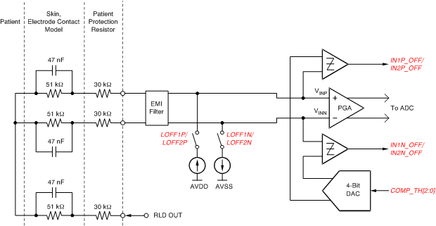
The basic principle is to inject an excitation signal and measure the response to find out if the electrode is off. As shown in the lead-off detection functional block diagram in Figure 37, this circuit provides two different methods of determining the state of the patient electrode. The methods differ in the frequency content of the excitation signal. Lead-off can be selectively done on a per channel basis using the LOFF_SENS register. Also, the internal excitation circuitry can be disabled and just the sensing circuitry can be enabled.
ADS1291 ADS1292 ADS1292R ai_lod_fbd_bas502.gif

NOTE:

The RP value must be selected in order to be below the maximum allowable current flow into a patient (in accordance with the relevant specification the latest revision of IEC 60601).
Figure 37. Lead-Off Detection