JAJSIY6C December   2011  – April 2020 ADS1291 , ADS1292 , ADS1292R

PRODUCTION DATA.  

  1. 特長
  2. アプリケーション
    1.     ブロック概略図
  3. 概要
  4. 改訂履歴
  5. Pin Configuration and Functions
    1.     Pin Functions
  6. Specifications
    1. 6.1 Absolute Maximum Ratings
    2. 6.2 ESD Ratings
    3. 6.3 Recommended Operating Conditions
    4. 6.4 Thermal Information
    5. 6.5 Electrical Characteristics
    6. 6.6 Timing Requirements
    7. 6.7 Typical Characteristics
  7. Parameter Measurement Information
    1. 7.1 Noise Measurements
  8. Detailed Description
    1. 8.1 Overview
    2. 8.2 Functional Block Diagram
    3. 8.3 Feature Description
      1. 8.3.1  EMI Filter
      2. 8.3.2  Input Multiplexer
        1. 8.3.2.1 Device Noise Measurements
        2. 8.3.2.2 Test Signals (TestP and TestN)
        3. 8.3.2.3 Auxiliary Differential Input (RESP_MODN/IN3N, RESP_MODN/IN3P)
        4. 8.3.2.4 Temperature Sensor (TEMPP, TEMPN)
        5. 8.3.2.5 Supply Measurements (MVDDP, MVDDN)
        6. 8.3.2.6 Lead-Off Excitation Signals (LoffP, LoffN)
        7. 8.3.2.7 Auxiliary Single-Ended Input
      3. 8.3.3  Analog Input
      4. 8.3.4  PGA Settings and Input Range
        1. 8.3.4.1 Input Common-Mode Range
        2. 8.3.4.2 Input Differential Dynamic Range
        3. 8.3.4.3 ADC ΔΣ Modulator
      5. 8.3.5  Digital Decimation Filter
        1. 8.3.5.1 Sinc Filter Stage (sinx / x)
      6. 8.3.6  Reference
      7. 8.3.7  Clock
      8. 8.3.8  Data Format
      9. 8.3.9  Multiple Device Configuration
        1. 8.3.9.1 Standard Mode
      10. 8.3.10 ECG-Specific Functions
        1. 8.3.10.1 Input Multiplexer (Rerouting the Right Leg Drive Signal)
          1. 8.3.10.1.1 Input Multiplexer (Measuring the Right Leg Drive Signal)
        2. 8.3.10.2 Lead-Off Detection
          1. 8.3.10.2.1 DC Lead-Off
          2. 8.3.10.2.2 AC Lead-Off
          3. 8.3.10.2.3 RLD Lead-Off
          4. 8.3.10.2.4 Right Leg Drive (RLD DC Bias Circuit)
            1. 8.3.10.2.4.1 RLD Configuration With Multiple Devices
        3. 8.3.10.3 PACE Detect
        4. 8.3.10.4 Respiration
          1. 8.3.10.4.1 Internal Respiration Circuitry With Internal Clock (ADS1292R)
          2. 8.3.10.4.2 Internal Respiration Circuitry With External Clock (ADS1292R)
      11. 8.3.11 Setting the Device for Basic Data Capture
        1. 8.3.11.1 Lead-Off
    4. 8.4 Device Functional Modes
    5. 8.5 Programming
      1. 8.5.1 SPI Interface
        1. 8.5.1.1  Chip Select (CS)
        2. 8.5.1.2  Serial Clock (SCLK)
        3. 8.5.1.3  Data Input (DIN)
        4. 8.5.1.4  Data Output (DOUT)
        5. 8.5.1.5  Data Retrieval
        6. 8.5.1.6  Data Ready (DRDY)
        7. 8.5.1.7  GPIO
        8. 8.5.1.8  Power-Down and Reset (PWDN/RESET)
        9. 8.5.1.9  START
        10. 8.5.1.10 Settling Time
        11. 8.5.1.11 Continuous Mode
        12. 8.5.1.12 Single-Shot Mode
      2. 8.5.2 SPI Command Definitions
        1. 8.5.2.1  WAKEUP: Exit STANDBY Mode
        2. 8.5.2.2  STANDBY: Enter STANDBY Mode
        3. 8.5.2.3  RESET: Reset Registers to Default Values
        4. 8.5.2.4  START: Start Conversions
        5. 8.5.2.5  STOP: Stop Conversions
        6. 8.5.2.6  OFFSETCAL: Channel Offset Calibration
        7. 8.5.2.7  RDATAC: Read Data Continuous
        8. 8.5.2.8  SDATAC: Stop Read Data Continuous
        9. 8.5.2.9  RDATA: Read Data
        10. 8.5.2.10 Sending Multi-Byte Commands
        11. 8.5.2.11 RREG: Read From Register
        12. 8.5.2.12 WREG: Write to Register
    6. 8.6 Register Maps
      1. 8.6.1 User Register Description
        1. 8.6.1.1  ID: ID Control Register (Factory-Programmed, Read-Only) (address = 00h)
          1. Table 17. ID: ID Control Register (Factory-Programmed, Read-Only) Field Descriptions
        2. 8.6.1.2  CONFIG1: Configuration Register 1 (address = 01h)
          1. Table 18. CONFIG1: Configuration Register 1 Field Descriptions
        3. 8.6.1.3  CONFIG2: Configuration Register 2 (address = 02h)
          1. Table 19. CONFIG2: Configuration Register 2 Field Descriptions
        4. 8.6.1.4  LOFF: Lead-Off Control Register (address = 03h)
          1. Table 20. LOFF: Lead-Off Control Register Field Descriptions
        5. 8.6.1.5  CH1SET: Channel 1 Settings (address = 04h)
          1. Table 21. CH1SET: Channel 1 Settings Field Descriptions
        6. 8.6.1.6  CH2SET: Channel 2 Settings (address = 05h)
          1. Table 22. CH2SET: Channel 2 Settings Field Descriptions
        7. 8.6.1.7  RLD_SENS: Right Leg Drive Sense Selection (address = 06h)
          1. Table 23. RLD_SENS: Right Leg Drive Sense Selection Field Descriptions
        8. 8.6.1.8  LOFF_SENS: Lead-Off Sense Selection (address = 07h)
          1. Table 24. LOFF_SENS: Lead-Off Sense Selection Field Descriptions
        9. 8.6.1.9  LOFF_STAT: Lead-Off Status (address = 08h)
          1. Table 25. LOFF_STAT: Lead-Off Status Field Descriptions
        10. 8.6.1.10 RESP1: Respiration Control Register 1 (address = 09h)
          1. Table 26. RESP1: Respiration Control Register 1 Field Descriptions
        11. 8.6.1.11 RESP2: Respiration Control Register 2 (address = 0Ah)
          1. Table 27. RESP2: Respiration Control Register 2 Field Descriptions
        12. 8.6.1.12 GPIO: General-Purpose I/O Register (address = 0Bh)
          1. Table 28. GPIO: General-Purpose I/O Register Field Descriptions
  9. Application and Implementation
    1. 9.1 Application Information
    2. 9.2 Typical Application
      1. 9.2.1 Design Requirements
      2. 9.2.2 Detailed Design Procedure
      3. 9.2.3 Application Curves
  10. 10Power Supply Recommendations
    1. 10.1 Power-Up Sequencing
  11. 11Layout
    1. 11.1 Layout Guidelines
      1. 11.1.1 PCB Layout
        1. 11.1.1.1 Power Supplies and Grounding
          1. 11.1.1.1.1 Connecting the Device to Unipolar (+3 V or +1.8 V) Supplies
          2. 11.1.1.1.2 Connecting the Device to Bipolar (±1.5 V or 1.8 V) Supplies
        2. 11.1.1.2 Shielding Analog Signal Paths
    2. 11.2 Layout Example
  12. 12デバイスおよびドキュメントのサポート
    1. 12.1 関連リンク
    2. 12.2 ドキュメントの更新通知を受け取る方法
    3. 12.3 サポート・リソース
    4. 12.4 商標
    5. 12.5 静電気放電に関する注意事項
    6. 12.6 Glossary
  13. 13メカニカル、パッケージ、および注文情報

Continuous Mode

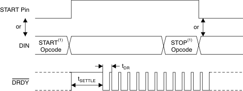
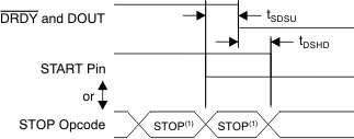
Conversions begin when the START pin is taken high or when the START opcode command is sent. As seen in Figure 49, the DRDY output goes high when conversions are started and goes low when data are ready. Conversions continue indefinitely until the START pin is taken low or the STOP opcode command is transmitted. When the START pin is pulled low or the stop command is issued, the conversion in progress is allowed to complete. Figure 50 and Table 14 show the required DRDY timing to the START pin and the START and STOP opcode commands when controlling conversions in this mode. To keep the converter running continuously, the START pin can be permanently tied high. Note that when switching from pulse mode to continuous mode, the START signal is pulsed or a STOP command must be issued, followed by a START command. This conversion mode is ideal for applications that require a fixed continuous stream of conversions results.
ADS1291 ADS1292 ADS1292R ai_tim_cont_conv_bas459.gif
START and STOP opcode commands take effect on the seventh SCLK falling edge.
Figure 49. Continuous Conversion Mode
ADS1291 ADS1292 ADS1292R ai_tim_start-drdy_bas459.gif
START and STOP commands take effect on the seventh SCLK falling edge at the end of the opcode transmission.
Figure 50. START to DRDY Timing

Table 14. Timing Characteristics for Figure 50(1)

PARAMETER MIN UNIT
tSDSU START pin low or STOP opcode to DRDY setup time to halt further conversions 8 tMOD
tDSHD START pin low or STOP opcode to complete current conversion 8 tMOD
START and STOP commands take effect on the seventh SCLK falling edge at the end of the opcode transmission.