JAJSJG4B August 2020 – May 2024 LP8864S-Q1
PRODUCTION DATA
- 1
- 1 特長
- 2 アプリケーション
- 3 概要
- 4 Pin Configuration and Functions
- 5 Specifications
-
6 Detailed Description
- 6.1 Overview
- 6.2 Functional Block Diagram
- 6.3
Feature Description
- 6.3.1 Control Interface
- 6.3.2 Function Setting
- 6.3.3 Device Supply (VDD)
- 6.3.4 Enable (EN)
- 6.3.5 Charge Pump
- 6.3.6 Boost Controller
- 6.3.7 LED Current Sinks
- 6.3.8 Brightness Control
- 6.3.9
Protection and Fault Detections
- 6.3.9.1 Supply Faults
- 6.3.9.2
Boost Faults
- 6.3.9.2.1 Boost Overvoltage Faults (BSTOVPL, BSTOVPH)
- 6.3.9.2.2 Boost Overcurrent Faults (BSTOCP)
- 6.3.9.2.3 LEDSET Resistor Missing Faults (LEDSET)
- 6.3.9.2.4 MODE Resistor Missing Faults (MODESEL)
- 6.3.9.2.5 FSET Resistor Missing Faults (FSET)
- 6.3.9.2.6 ISET Resistor Out of Range Faults (ISET)
- 6.3.9.2.7 Thermal Shutdown Faults (TSD)
- 6.3.9.3 LED Faults
- 6.3.9.4 Overview of the Fault and Protection Schemes
- 6.4 Device Functional Modes
- 6.5 Programming
- 7 Register Maps
-
8 Application and Implementation
- 8.1 Application Information
- 8.2
Typical Applications
- 8.2.1
Full Feature Application for Display Backlight
- 8.2.1.1 Design Requirements
- 8.2.1.2
Detailed Design Procedure
- 8.2.1.2.1 Inductor Selection
- 8.2.1.2.2 Output Capacitor Selection
- 8.2.1.2.3 Input Capacitor Selection
- 8.2.1.2.4 Charge Pump Output Capacitor
- 8.2.1.2.5 Charge Pump Flying Capacitor
- 8.2.1.2.6 Output Diode
- 8.2.1.2.7 Switching FET
- 8.2.1.2.8 Boost Sense Resistor
- 8.2.1.2.9 Power-Line FET
- 8.2.1.2.10 Input Current Sense Resistor
- 8.2.1.2.11 Feedback Resistor Divider
- 8.2.1.2.12 Critical Components for Design
- 8.2.1.3 Application Curves
- 8.2.2 Application with Basic/Minimal Operation
- 8.2.3
SEPIC Mode Application
- 8.2.3.1 Design Requirements
- 8.2.3.2
Detailed Design Procedure
- 8.2.3.2.1 Inductor Selection
- 8.2.3.2.2 Coupling Capacitor Selection
- 8.2.3.2.3 Output Capacitor Selection
- 8.2.3.2.4 Input Capacitor Selection
- 8.2.3.2.5 Charge Pump Output Capacitor
- 8.2.3.2.6 Charge Pump Flying Capacitor
- 8.2.3.2.7 Switching FET
- 8.2.3.2.8 Output Diode
- 8.2.3.2.9 Switching Sense Resistor
- 8.2.3.2.10 Power-Line FET
- 8.2.3.2.11 Input Current Sense Resistor
- 8.2.3.2.12 Feedback Resistor Divider
- 8.2.3.2.13 Critical Components for Design
- 8.2.3.3 Application Curves
- 8.2.1
Full Feature Application for Display Backlight
- 8.3 Power Supply Recommendations
- 8.4 Layout
- 9 Device and Documentation Support
- 10Revision History
- 11Mechanical, Packaging, and Orderable Information
6.3.8.5 Hybrid Mode
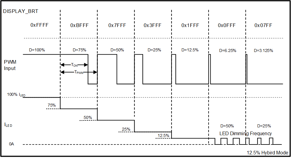
In addition to phase-shift PWM dimming, LP8864S-Q1 supports a hybrid-dimming mode. Hybrid dimming combines PWM and current modes for brightness control for the display brightness path. By using hybrid dimming, dimming ratio could be increased by another 8 times. In hybrid mode, PWM dimming is used for low brightness range of brightness, and current dimming is used for high brightness levels as shown in Figure 6-11. Current dimming control enables improved optical efficiency due to increased LED efficiency at lower currents. PWM dimming control at low brightness levels ensures linear and accurate control. Hybrid mode can be selected through resistor value at MODE pin as Table 6-7. The PWM and current modes transition threshold can be set at 12.5% or at 0% brightness. The latter selection allows for pure current dimming control mode.
 Figure 6-11 Hybrid Dimming Diagram