JAJSJG4B August 2020 – May 2024 LP8864S-Q1
PRODUCTION DATA
- 1
- 1 特長
- 2 アプリケーション
- 3 概要
- 4 Pin Configuration and Functions
- 5 Specifications
-
6 Detailed Description
- 6.1 Overview
- 6.2 Functional Block Diagram
- 6.3
Feature Description
- 6.3.1 Control Interface
- 6.3.2 Function Setting
- 6.3.3 Device Supply (VDD)
- 6.3.4 Enable (EN)
- 6.3.5 Charge Pump
- 6.3.6 Boost Controller
- 6.3.7 LED Current Sinks
- 6.3.8 Brightness Control
- 6.3.9
Protection and Fault Detections
- 6.3.9.1 Supply Faults
- 6.3.9.2
Boost Faults
- 6.3.9.2.1 Boost Overvoltage Faults (BSTOVPL, BSTOVPH)
- 6.3.9.2.2 Boost Overcurrent Faults (BSTOCP)
- 6.3.9.2.3 LEDSET Resistor Missing Faults (LEDSET)
- 6.3.9.2.4 MODE Resistor Missing Faults (MODESEL)
- 6.3.9.2.5 FSET Resistor Missing Faults (FSET)
- 6.3.9.2.6 ISET Resistor Out of Range Faults (ISET)
- 6.3.9.2.7 Thermal Shutdown Faults (TSD)
- 6.3.9.3 LED Faults
- 6.3.9.4 Overview of the Fault and Protection Schemes
- 6.4 Device Functional Modes
- 6.5 Programming
- 7 Register Maps
-
8 Application and Implementation
- 8.1 Application Information
- 8.2
Typical Applications
- 8.2.1
Full Feature Application for Display Backlight
- 8.2.1.1 Design Requirements
- 8.2.1.2
Detailed Design Procedure
- 8.2.1.2.1 Inductor Selection
- 8.2.1.2.2 Output Capacitor Selection
- 8.2.1.2.3 Input Capacitor Selection
- 8.2.1.2.4 Charge Pump Output Capacitor
- 8.2.1.2.5 Charge Pump Flying Capacitor
- 8.2.1.2.6 Output Diode
- 8.2.1.2.7 Switching FET
- 8.2.1.2.8 Boost Sense Resistor
- 8.2.1.2.9 Power-Line FET
- 8.2.1.2.10 Input Current Sense Resistor
- 8.2.1.2.11 Feedback Resistor Divider
- 8.2.1.2.12 Critical Components for Design
- 8.2.1.3 Application Curves
- 8.2.2 Application with Basic/Minimal Operation
- 8.2.3
SEPIC Mode Application
- 8.2.3.1 Design Requirements
- 8.2.3.2
Detailed Design Procedure
- 8.2.3.2.1 Inductor Selection
- 8.2.3.2.2 Coupling Capacitor Selection
- 8.2.3.2.3 Output Capacitor Selection
- 8.2.3.2.4 Input Capacitor Selection
- 8.2.3.2.5 Charge Pump Output Capacitor
- 8.2.3.2.6 Charge Pump Flying Capacitor
- 8.2.3.2.7 Switching FET
- 8.2.3.2.8 Output Diode
- 8.2.3.2.9 Switching Sense Resistor
- 8.2.3.2.10 Power-Line FET
- 8.2.3.2.11 Input Current Sense Resistor
- 8.2.3.2.12 Feedback Resistor Divider
- 8.2.3.2.13 Critical Components for Design
- 8.2.3.3 Application Curves
- 8.2.1
Full Feature Application for Display Backlight
- 8.3 Power Supply Recommendations
- 8.4 Layout
- 9 Device and Documentation Support
- 10Revision History
- 11Mechanical, Packaging, and Orderable Information
6.3.5 Charge Pump
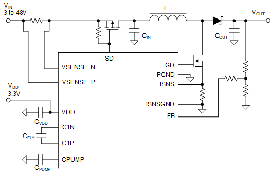
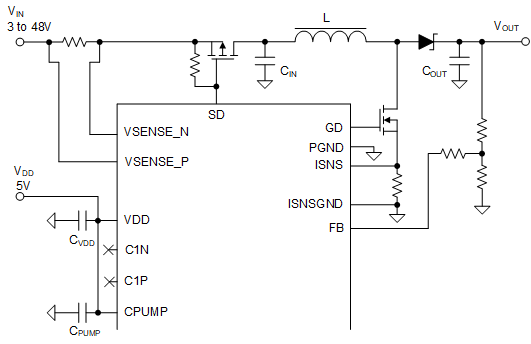
An integrated regulated charge pump can be used to supply the gate drive for the external FET of the boost controller. The charge pump is enabled or disabled by automatically detecting whether VDD and CPUMP pin are connected together. If VDD is < 4.5V then use the charge pump to generate a 5V gate voltage to drive the external boost switching FET. To use the charge pump, a 2.2µF capacitor is placed between C1N and C1P. If the charge pump is not required, C1N and C1P could be left unconnected and CPUMP pins tied to VDD. A 4.7µF CPUMP capacitor is used to store energy for the gate driver. The CPUMP capacitor is required to be used in both charge pump enabled and disabled conditions and must be placed as close as possible to the CPUMP pins. Figure 6-1and Figure 6-2 show required connections for both use cases.
 Figure 6-1 Charge Pump Enabled
Circuit
 Figure 6-2 Charge Pump Disabled
Circuit
Figure 6-2 Charge Pump Disabled
CircuitIf the charge pump is enabled, the CPCAP_STATUS bit shows whether a fly capacitor was detected and the CP_STATUS bit shows status of any charge pump faults and generates an INT signal. The CP_INT_EN bit can be used to prevent the charge-pump fault from causing an interrupt on the INT pin.