JAJSJI9F July 2020 – July 2024 TMUX7208 , TMUX7209
PRODUCTION DATA
- 1
- 1 特長
- 2 アプリケーション
- 3 概要
- 4 Device Comparison Table
- 5 Pin Configuration and Functions
-
6 Specifications
- 6.1 Absolute Maximum Ratings
- 6.2 ESD Ratings
- 6.3 Thermal Information
- 6.4 Recommended Operating Conditions
- 6.5 Source or Drain Continuous Current
- 6.6 ±15 V Dual Supply: Electrical Characteristics
- 6.7 ±15 V Dual Supply: Switching Characteristics
- 6.8 ±20 V Dual Supply: Electrical Characteristics
- 6.9 ±20 V Dual Supply: Switching Characteristics
- 6.10 44 V Single Supply: Electrical Characteristics
- 6.11 44 V Single Supply: Switching Characteristics
- 6.12 12 V Single Supply: Electrical Characteristics
- 6.13 12 V Single Supply: Switching Characteristics
- 6.14 Typical Characteristics
-
7 Parameter Measurement Information
- 7.1 On-Resistance
- 7.2 Off-Leakage Current
- 7.3 On-Leakage Current
- 7.4 Transition Time
- 7.5 tON(EN) and tOFF(EN)
- 7.6 Break-Before-Make
- 7.7 tON (VDD) Time
- 7.8 Propagation Delay
- 7.9 Charge Injection
- 7.10 Off Isolation
- 7.11 Crosstalk
- 7.12 Bandwidth
- 7.13 THD + Noise
- 7.14 Power Supply Rejection Ratio (PSRR)
- 8 Detailed Description
- 9 Application and Implementation
- 10Device and Documentation Support
- 11Revision History
- 12Mechanical, Packaging, and Orderable Information
5 Pin Configuration and Functions
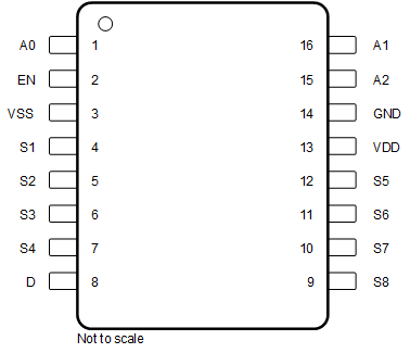
 Figure 5-1 TMUX7208: PW Package16-Pin TSSOPTop View
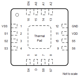
 Figure 5-2 TMUX7208: RUM
Package16-Pin WQFNTop View
Figure 5-2 TMUX7208: RUM
Package16-Pin WQFNTop ViewTable 5-1 TMUX7208 Pin
Functions
| PIN | TYPE(1) | DESCRIPTION(2) | ||
|---|---|---|---|---|
| NAME | PW | RUM | ||
| A0 | 1 | 15 | I | Logic control input, has internal 4MΩ pull-down resistor. Controls the switch configuration as shown in Section 8.5. |
| A1 | 16 | 14 | I | Logic control input, has internal 4MΩ pull-down resistor. Controls the switch configuration as shown in Section 8.5. |
| A2 | 15 | 13 | I | Logic control input, has internal 4MΩ pull-down resistor. Controls the switch configuration as shown in Section 8.5. |
| D | 8 | 6 | I/O | Drain pin. Can be an input or output. |
| EN | 2 | 16 | I | Active high logic enable, has internal 4MΩ pull-down resistor. When this pin is low, all switches are turned off. When this pin is high, the Ax logic input determines which switch is turned on. |
| GND | 14 | 12 | P | Ground (0V) reference. |
| S1 | 4 | 2 | I/O | Source pin 1. Can be an input or output. |
| S2 | 5 | 3 | I/O | Source pin 2. Can be an input or output. |
| S3 | 6 | 4 | I/O | Source pin 3. Can be an input or output. |
| S4 | 7 | 5 | I/O | Source pin 4. Can be an input or output. |
| S5 | 12 | 10 | I/O | Source pin 5. Can be an input or output. |
| S6 | 11 | 9 | I/O | Source pin 6. Can be an input or output. |
| S7 | 10 | 8 | I/O | Source pin 7. Can be an input or output. |
| S8 | 9 | 7 | I/O | Source pin 8. Can be an input or output. |
| VDD | 13 | 11 | P | Positive power supply. This pin is the most positive power-supply potential. For reliable operation, connect a decoupling capacitor ranging from 0.1μF to 10μF between VDD and GND. |
| VSS | 3 | 1 | P | Negative power supply. This pin is the most negative power-supply potential. In single-supply applications, this pin can be connected to ground. For reliable operation, connect a decoupling capacitor ranging from 0.1μF to 10μF between VSS and GND. |
| Thermal Pad | — | The thermal pad is not connected internally. It is recommended that the pad be tied to GND or VSS for best performance. | ||
(1) I = input, O = output, I/O = input and output, P = power.
(2) Refer to Section 8.4 for what to do with
unused pins.
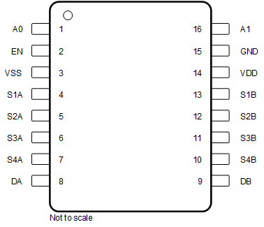
 Figure 5-3 TMUX7209: PW
Package16-Pin TSSOPTop View
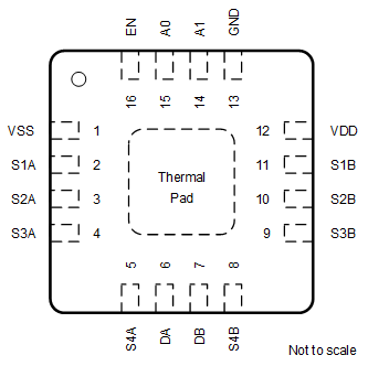
 Figure 5-4 TMUX7209: RUM
Package16-Pin WQFNTop View
Figure 5-4 TMUX7209: RUM
Package16-Pin WQFNTop ViewTable 5-2 TMUX7209 Pin Functions
| PIN | TYPE(1) | DESCRIPTION(2) | ||
|---|---|---|---|---|
| NAME | PW | RUM | ||
| A0 | 1 | 15 | I | Logic control input, has internal pull-down resistor. Controls the switch configuration as shown in Section 8.5. |
| A1 | 16 | 14 | I | Logic control input, has internal pull-down resistor. Controls the switch configuration as shown in Section 8.5. |
| DA | 8 | 6 | I/O | Drain Terminal A. Can be an input or an output. |
| DB | 9 | 7 | I/O | Drain Terminal B. Can be an input or an output. |
| EN | 2 | 16 | I | Active high logic enable, has internal pull-up resistor. When this pin is low, all switches are turned off. When this pin is high, the Ax logic input determines which switch is turned on. |
| GND | 15 | 13 | P | Ground (0V) reference. |
| S1A | 4 | 2 | I/O | Source pin 1A. Can be an input or output. |
| S1B | 13 | 11 | I/O | Source pin 1B. Can be an input or output. |
| S2A | 5 | 3 | I/O | Source pin 2A. Can be an input or output. |
| S2B | 12 | 10 | I/O | Source pin 2B. Can be an input or output. |
| S3A | 6 | 4 | I/O | Source pin 3A. Can be an input or output. |
| S3B | 11 | 9 | I/O | Source pin 3B. Can be an input or output. |
| S4A | 7 | 5 | I/O | Source pin 4A. Can be an input or output. |
| S4B | 10 | 8 | I/O | Source pin 4B. Can be an input or output. |
| VDD | 14 | 12 | P | Positive power supply. This pin is the most positive power-supply potential. For reliable operation, connect a decoupling capacitor ranging from 0.1μF to 10μF between VDD and GND. |
| VSS | 3 | 1 | P | Negative power supply. This pin is the most negative power-supply potential. In single-supply applications, this pin can be connected to ground. For reliable operation, connect a decoupling capacitor ranging from 0.1μF to 10μF between VSS and GND. |
| Thermal Pad | — | The thermal pad is not connected internally. It is recommended that the pad be tied to GND or VSS for best performance. | ||
(1) I = input, O = output, I/O =
input and output, P = power.
(2) Refer to Section 8.4 for what to do with
unused pins.