JAJSJQ9C September 2021 – April 2022 ISOW7740 , ISOW7741 , ISOW7742 , ISOW7743 , ISOW7744
PRODUCTION DATA
- 1 特長
- 2 アプリケーション
- 3 概要
- 4 Revision History
- 5 概要 (続き)
- 6 Pin Configuration and Functions
-
7 Specifications
- 7.1 Absolute Maximum Ratings
- 7.2 ESD Ratings
- 7.3 Recommended Operating Conditions
- 7.4 Thermal Information
- 7.5 Power Ratings
- 7.6 Insulation Specifications
- 7.7 Safety-Related Certifications
- 7.8 Safety Limiting Values
- 7.9 Electrical Characteristics - Power Converter
- 7.10 Supply Current Characteristics - Power Converter
- 7.11 Electrical Characteristics Channel Isolator - VIO, VISOIN = 5-V
- 7.12 Supply Current Characteristics Channel Isolator - VIO, VISOIN = 5-V
- 7.13 Electrical Characteristics Channel Isolator - VIO, VISOIN = 3.3-V
- 7.14 Supply Current Characteristics Channel Isolator - VIO, VISOIN = 3.3-V
- 7.15 Electrical Characteristics Channel Isolator - VIO, VISOIN = 2.5-V
- 7.16 Supply Current Characteristics Channel Isolator - VIO, VISOIN = 2.5-V
- 7.17 Electrical Characteristics Channel Isolator - VIO, VISOIN = 1.8-V
- 7.18 Supply Current Characteristics Channel Isolator - VIO, VISOIN = 1.8-V
- 7.19 Switching Characteristics - 5-V Supply
- 7.20 Switching Characteristics - 3.3-V Supply
- 7.21 Switching Characteristics - 2.5-V Supply
- 7.22 Switching Characteristics - 1.8-V Supply
- 7.23 Insulation Characteristics Curves
- 7.24 Typical Characteristics
- 8 Parameter Measurement Information
- 9 Detailed Description
- 10Application and Implementation
- 11Power Supply Recommendations
- 12Layout
- 13Device and Documentation Support
- 14Mechanical, Packaging, and Orderable Information
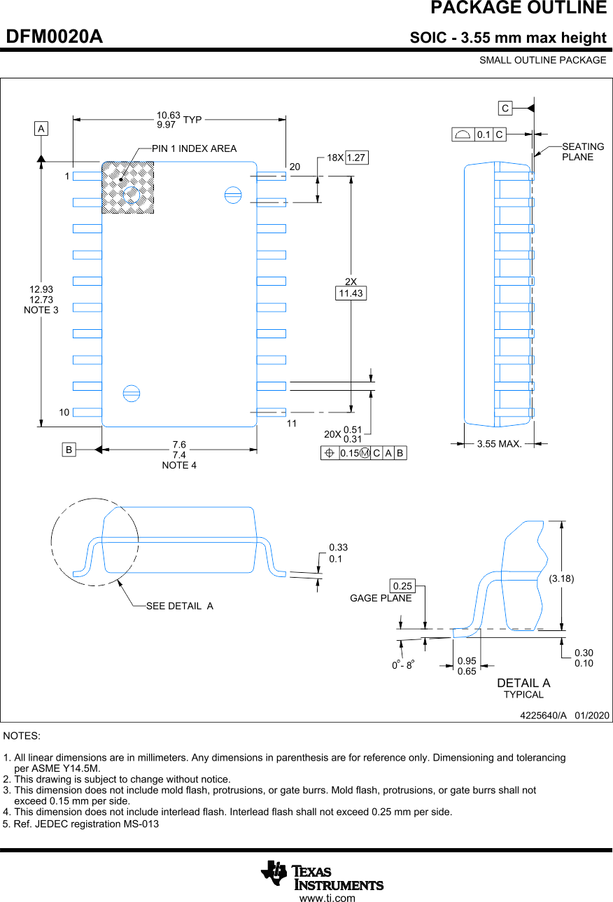
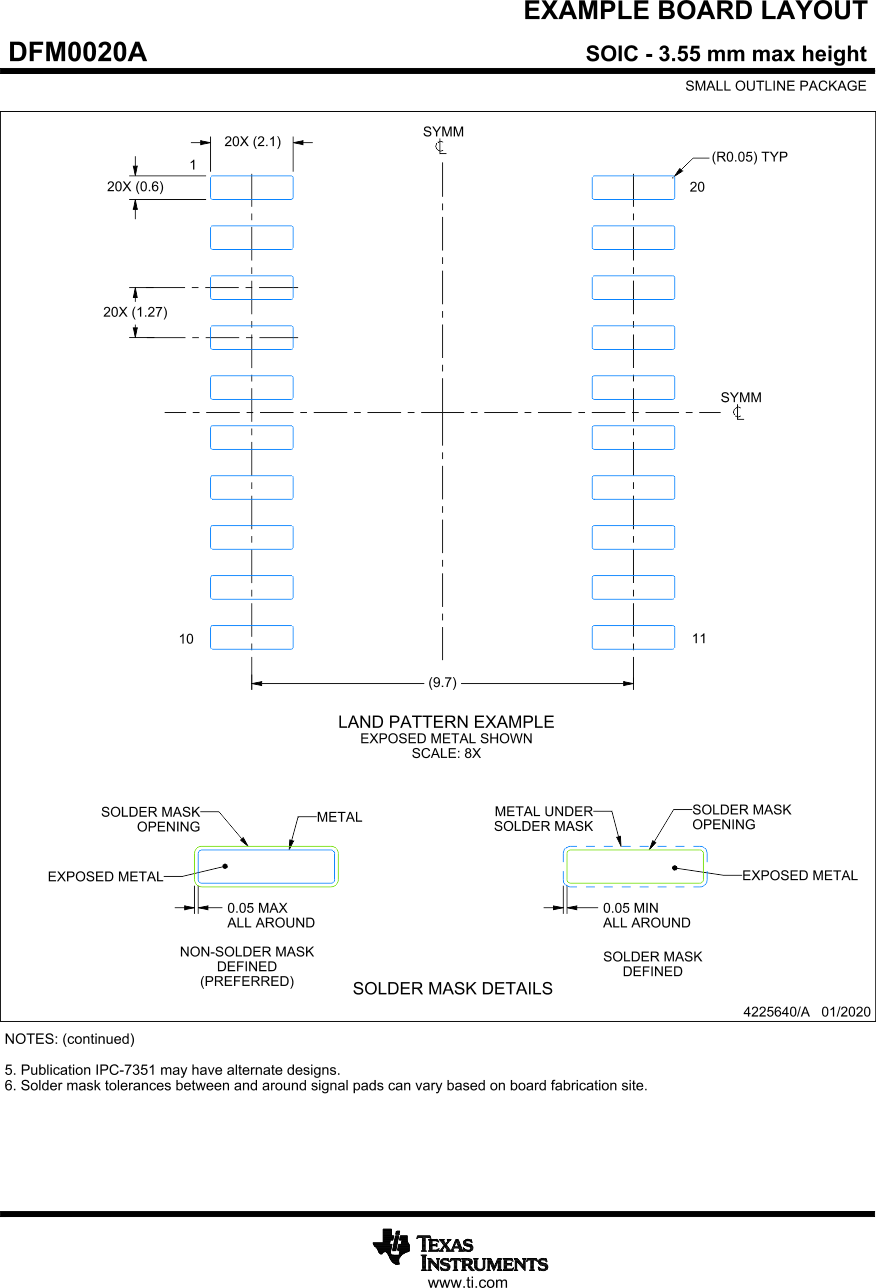
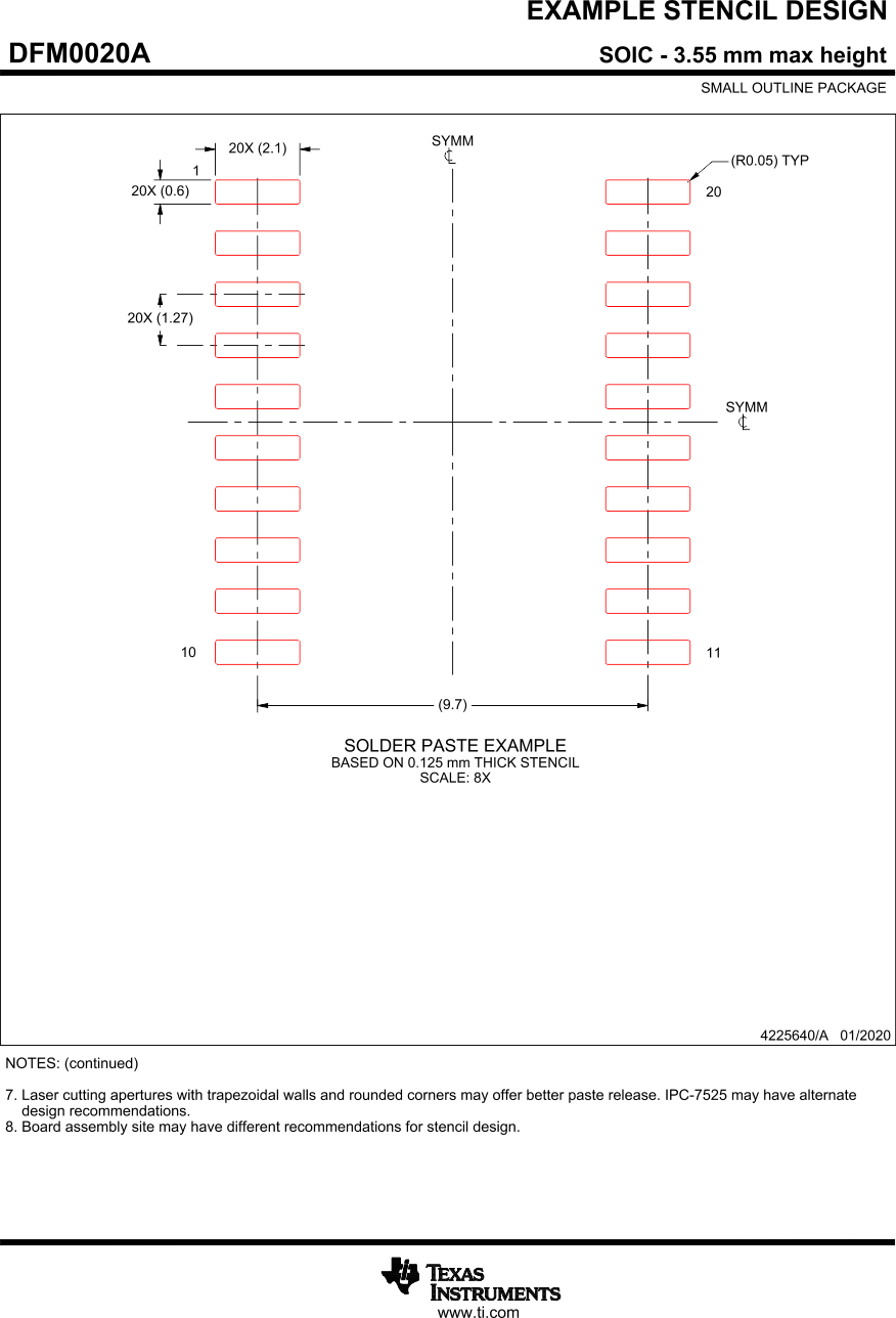
14 Mechanical, Packaging, and Orderable Information
The following pages include mechanical, packaging, and orderable information. This information is the most current data available for the designated devices. This data is subject to change without notice and revision of this document. For browser-based versions of this data sheet, refer to the left-hand navigation.


