JAJSJW0E September 2020 – July 2024 TMUX6219
PRODUCTION DATA
- 1
- 1 特長
- 2 アプリケーション
- 3 概要
- 4 Pin Configuration and Functions
-
5 Specifications
- 5.1 Absolute Maximum Ratings
- 5.2 ESD Ratings
- 5.3 Thermal Information
- 5.4 Recommended Operating Conditions
- 5.5 Source or Drain Continuous Current
- 5.6 ±15 V Dual Supply: Electrical Characteristics
- 5.7 ±15 V Dual Supply: Switching Characteristics
- 5.8 36 V Single Supply: Electrical Characteristics
- 5.9 36 V Single Supply: Switching Characteristics
- 5.10 12 V Single Supply: Electrical Characteristics
- 5.11 12 V Single Supply: Switching Characteristics
- 5.12 +5 V / -8 V Dual Supply: Electrical Characteristics
- 5.13 +5 V / -8 V Dual Supply: Switching Characteristics
- 5.14 ±5 V Dual Supply: Electrical Characteristics
- 5.15 ±5 V Dual Supply: Switching Characteristics
- 5.16 Typical Characteristics
-
6 Parameter Measurement Information
- 6.1 On-Resistance
- 6.2 Off-Leakage Current
- 6.3 On-Leakage Current
- 6.4 Transition Time
- 6.5 tON(EN) and tOFF(EN)
- 6.6 Break-Before-Make
- 6.7 tON (VDD) Time
- 6.8 Propagation Delay
- 6.9 Charge Injection
- 6.10 Off Isolation
- 6.11 Crosstalk
- 6.12 Bandwidth
- 6.13 THD + Noise
- 6.14 Power Supply Rejection Ratio (PSRR)
- 7 Detailed Description
- 8 Application and Implementation
- 9 Power Supply Recommendations
- 10Layout
- 11Device and Documentation Support
- 12Revision History
- 13Mechanical, Packaging, and Orderable Information
6.2 Off-Leakage Current
There are two types of leakage currents associated with a switch during the off state:
- Source off-leakage current.
- Drain off-leakage current.
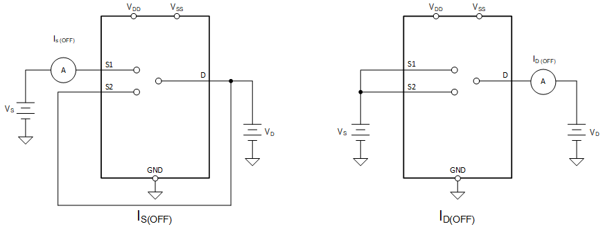
Source leakage current is defined as the leakage current flowing into or out of the source pin when the switch is off. This current is denoted by the symbol IS(OFF).
Drain leakage current is defined as the leakage current flowing into or out of the drain pin when the switch is off. This current is denoted by the symbol ID(OFF).
Figure 6-2 shows the setup used to measure both off-leakage currents.
 Figure 6-2 Off-Leakage Measurement Setup