JAJSJW0E September 2020 – July 2024 TMUX6219
PRODUCTION DATA
- 1
- 1 特長
- 2 アプリケーション
- 3 概要
- 4 Pin Configuration and Functions
-
5 Specifications
- 5.1 Absolute Maximum Ratings
- 5.2 ESD Ratings
- 5.3 Thermal Information
- 5.4 Recommended Operating Conditions
- 5.5 Source or Drain Continuous Current
- 5.6 ±15 V Dual Supply: Electrical Characteristics
- 5.7 ±15 V Dual Supply: Switching Characteristics
- 5.8 36 V Single Supply: Electrical Characteristics
- 5.9 36 V Single Supply: Switching Characteristics
- 5.10 12 V Single Supply: Electrical Characteristics
- 5.11 12 V Single Supply: Switching Characteristics
- 5.12 +5 V / -8 V Dual Supply: Electrical Characteristics
- 5.13 +5 V / -8 V Dual Supply: Switching Characteristics
- 5.14 ±5 V Dual Supply: Electrical Characteristics
- 5.15 ±5 V Dual Supply: Switching Characteristics
- 5.16 Typical Characteristics
-
6 Parameter Measurement Information
- 6.1 On-Resistance
- 6.2 Off-Leakage Current
- 6.3 On-Leakage Current
- 6.4 Transition Time
- 6.5 tON(EN) and tOFF(EN)
- 6.6 Break-Before-Make
- 6.7 tON (VDD) Time
- 6.8 Propagation Delay
- 6.9 Charge Injection
- 6.10 Off Isolation
- 6.11 Crosstalk
- 6.12 Bandwidth
- 6.13 THD + Noise
- 6.14 Power Supply Rejection Ratio (PSRR)
- 7 Detailed Description
- 8 Application and Implementation
- 9 Power Supply Recommendations
- 10Layout
- 11Device and Documentation Support
- 12Revision History
- 13Mechanical, Packaging, and Orderable Information
6.1 On-Resistance
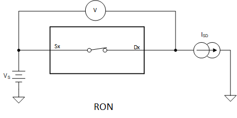
The on-resistance of a device is the ohmic resistance between the source (Sx) and drain (D) pins of the device. The on-resistance varies with input voltage and supply voltage. The symbol RON is used to denote on-resistance. Figure 6-1 shows the measurement setup used to measure RON. Voltage (V) and current (ISD) are measured using the following setup, where RON is computed as RON = V / ISD:
 Figure 6-1 On-Resistance