JAJSKH4A April   2022  – May 2024 TUSB1104

PRODUCTION DATA  

  1.   1
  2. 特長
  3. アプリケーション
  4.   概要
  5. Pin Configuration and Functions
  6. Specifications
    1. 4.1  Absolute Maximum Ratings
    2. 4.2  ESD Ratings
    3. 4.3  Recommended Operating Conditions
    4. 4.4  Thermal Information
    5. 4.5  Power Supply Characteristics
    6. 4.6  Control I/O DC Electrical Characteristics
    7. 4.7  USB Electrical Characteristics
    8. 4.8  Timing Requirements
    9. 4.9  Switching Characteristics
    10. 4.10 Typical Characteristics
  7. Parameter Measurement Information
  8. Detailed Description
    1. 6.1 Overview
    2. 6.2 Functional Block Diagram
    3. 6.3 Feature Description
      1. 6.3.1 4-Level Inputs
      2. 6.3.2 USB Receiver Linear Equalization
        1. 6.3.2.1 Linear EQ Configuration
        2. 6.3.2.2 Full Adaptive Equalization
        3. 6.3.2.3 Fast Adaptive Equalization
      3. 6.3.3 USB Transmitter
        1. 6.3.3.1 Linearity VOD
        2. 6.3.3.2 Limited VOD
        3. 6.3.3.3 Transmit Equalization (Limited Redriver Mode Only)
      4. 6.3.4 USB 3.2 x2 Description
      5. 6.3.5 USB Polarity Inversion
      6. 6.3.6 Receiver Detect Control
    4. 6.4 Device Functional Modes
      1. 6.4.1 MODE Pin
      2. 6.4.2 Rx EQ Configuration in Pin-Strap Mode
      3. 6.4.3 USB 3.2 Power States
      4. 6.4.4 Disabling U1 and U2
    5. 6.5 Programming
      1. 6.5.1 Pseudocode Examples
        1. 6.5.1.1 Fixed EQ with Linear Redriver Mode
        2. 6.5.1.2 Fixed EQ with Limited Redriver Mode
        3. 6.5.1.3 Fast AEQ with Linear Redriver Mode
        4. 6.5.1.4 Fast AEQ with Limited Redriver Mode
        5. 6.5.1.5 Full AEQ with Linear Redriver Mode
        6. 6.5.1.6 Full AEQ with Limited Redriver Mode
      2. 6.5.2 TUSB1104 I2C Address Options
      3. 6.5.3 TUSB1104 I2C Target Behavior
    6. 6.6 Register Map
      1. 6.6.1 Device Registers
  9. Application and Implementation
    1. 7.1 Application Information
    2. 7.2 Typical Application
      1. 7.2.1 Design Requirements
      2. 7.2.2 Detailed Design Procedure
        1. 7.2.2.1 USB SSTX1/2 Receiver Configuration
        2. 7.2.2.2 USB CRX1/2 Receiver Configuration
          1. 7.2.2.2.1 Fixed Equalization
          2. 7.2.2.2.2 Full Adaptive Equalization
          3. 7.2.2.2.3 Fast Adaptive Equalization
        3. 7.2.2.3 ESD Protection
      3. 7.2.3 Application Curves
    3. 7.3 Power Supply Recommendations
    4. 7.4 Layout
      1. 7.4.1 Layout Guidelines
      2. 7.4.2 Layout Example
  10. Device and Documentation Support
    1. 8.1 ドキュメントの更新通知を受け取る方法
    2. 8.2 サポート・リソース
    3. 8.3 Trademarks
    4. 8.4 静電気放電に関する注意事項
    5. 8.5 用語集
  11. Revision History
  12. 10Mechanical, Packaging, and Orderable Information

Detailed Design Procedure

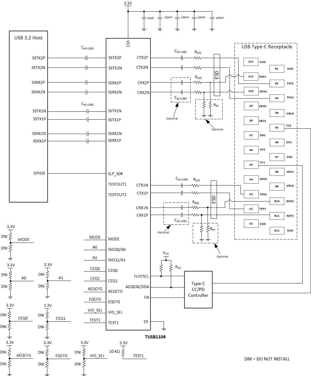
A typical usage of the TUSB1104 device is shown in Figure 7-2. The device can be configure either through its GPIO pins or through its I2C interface. In the following example, a Type-C PD controller or microcontroller is used to configure the device through the I2C interface. In I2C mode, the equalization settings for each receiver can be independently controlled through I2C registers. For this reason, all of the equalization pins (SSEQ[1:0], and CEQ[1:0]) can be left unconnected. If these pins are left unconnected, the TUSB1104 7-bit I2C target address will be 0x12 because both SSEQ1/A1 and SSEQ0/A0 will be at pin level F. If a different I2C target address is desired, SSEQ1/A1 and SSEQ0/A0 pins should be set to a level which produces the desired I2C target address.
TUSB1104 Application Circuit Figure 7-2 Application Circuit