JAJSKH8A December 2020 – June 2021 TLV320ADC6120
PRODUCTION DATA
- 1 特長
- 2 アプリケーション
- 3 概要
- 4 Revision History
- 5 Device Comparison Table
- 6 Pin Configuration and Functions
-
7 Specifications
- 7.1 Absolute Maximum Ratings
- 7.2 ESD Ratings
- 7.3 Recommended Operating Conditions
- 7.4 Thermal Information
- 7.5 Electrical Characteristics
- 7.6 Timing Requirements: I2C Interface
- 7.7 Switching Characteristics: I2C Interface
- 7.8 Timing Requirements: TDM, I2S or LJ Interface
- 7.9 Switching Characteristics: TDM, I2S or LJ Interface
- 7.10 Timing Requirements: PDM Digital Microphone Interface
- 7.11 Switching Characteristics: PDM Digital Microphone Interface
- 7.12 Timing Diagrams
- 7.13 Typical Characteristics
-
8 Detailed Description
- 8.1 Overview
- 8.2 Functional Block Diagram
- 8.3
Feature Description
- 8.3.1 Serial Interfaces
- 8.3.2 Phase-Locked Loop (PLL) and Clock Generation
- 8.3.3 Input Channel Configurations
- 8.3.4 Reference Voltage
- 8.3.5 Programmable Microphone Bias
- 8.3.6
Signal-Chain Processing
- 8.3.6.1 Programmable Channel Gain and Digital Volume Control
- 8.3.6.2 Programmable Channel Gain Calibration
- 8.3.6.3 Programmable Channel Phase Calibration
- 8.3.6.4 Programmable Digital High-Pass Filter
- 8.3.6.5 Programmable Digital Biquad Filters
- 8.3.6.6 Programmable Channel Summer and Digital Mixer
- 8.3.6.7
Configurable Digital Decimation Filters
- 8.3.6.7.1
Linear Phase Filters
- 8.3.6.7.1.1 Sampling Rate: 7.35 kHz to 8 kHz
- 8.3.6.7.1.2 Sampling Rate: 14.7 kHz to 16 kHz
- 8.3.6.7.1.3 Sampling Rate: 22.05 kHz to 24 kHz
- 8.3.6.7.1.4 Sampling Rate: 29.4 kHz to 32 kHz
- 8.3.6.7.1.5 Sampling Rate: 44.1 kHz to 48 kHz
- 8.3.6.7.1.6 Sampling Rate: 88.2 kHz to 96 kHz
- 8.3.6.7.1.7 Sampling Rate: 176.4 kHz to 192 kHz
- 8.3.6.7.1.8 Sampling Rate: 352.8 kHz to 384 kHz
- 8.3.6.7.1.9 Sampling Rate: 705.6 kHz to 768 kHz
- 8.3.6.7.2 Low-Latency Filters
- 8.3.6.7.3
Ultra-Low Latency Filters
- 8.3.6.7.3.1 Sampling Rate: 14.7 kHz to 16 kHz
- 8.3.6.7.3.2 Sampling Rate: 22.05 kHz to 24 kHz
- 8.3.6.7.3.3 Sampling Rate: 29.4 kHz to 32 kHz
- 8.3.6.7.3.4 Sampling Rate: 44.1 kHz to 48 kHz
- 8.3.6.7.3.5 Sampling Rate: 88.2 kHz to 96 kHz
- 8.3.6.7.3.6 Sampling Rate: 176.4 kHz to 192 kHz
- 8.3.6.7.3.7 Sampling Rate: 352.8 kHz to 384 kHz
- 8.3.6.7.1
Linear Phase Filters
- 8.3.7 Dynamic Range Enhancer (DRE)
- 8.3.8 Dynamic Range Compressor (DRC)
- 8.3.9 Automatic Gain Controller (AGC)
- 8.3.10 Voice Activity Detection (VAD)
- 8.3.11 Digital PDM Microphone Record Channel
- 8.3.12 Interrupts, Status, and Digital I/O Pin Multiplexing
- 8.4 Device Functional Modes
- 8.5 Programming
- 8.6 Register Maps
- 9 Application and Implementation
- 10Power Supply Recommendations
- 11Layout
- 12Device and Documentation Support
- 13Mechanical, Packaging, and Orderable Information
8.3.11 Digital PDM Microphone Record Channel
In addition to supporting analog microphones, the device also interfaces to digital pulse-density-modulation (PDM) microphones and uses high-order and high-performance decimation filters to generate pulse code modulation (PCM) output data that can be transmitted on the audio serial interface to the host. The device supports up to four digital microphone recording channels. If the second channel analog microphone is not used in the system, then the analog input pins (IN2P and IN2M) can be repurposed as the GPI1 and GPO1 pins, respectively, and can be configured for the PDMDIN1 and PDMCLK clocks for digital PDM microphone recording. GPIO1 or GPI2 (multiplexed with MICBIAS) can be used as PDMDIN2 to enable four-channel PDM microphone recording. If two-channel analog input recording is needed, MICBIAS (configured as GPI2) and GPIO1 can be used as PDMDIN and PDMCLK, respectively, to enable two-channel DMIC recording along with two-channel AIN recording. The device can support a total of four channels at the input (analog and digital).
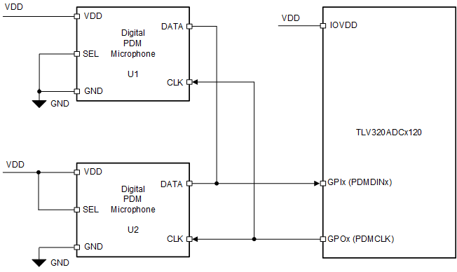
The device internally generates PDMCLK with a programmable frequency of either 6.144 MHz, 3.072 MHz, 1.536 MHz, or 768 kHz (for output data sample rates in multiples or submultiples of 48 kHz) or 5.6448 MHz, 2.8224 MHz, 1.4112 MHz, or 705.6 kHz (for output data sample rates in multiples or submultiples of 44.1 kHz) using the PDMCLK_DIV[1:0] (P0_R31_D[1:0]) register bits. PDMCLK can be routed on the GPO1 and GPIO1 pins. This clock can be connected to the external digital microphone device. Figure 8-64 shows a connection diagram of the digital PDM microphones.
 Figure 8-64 Digital
PDM Microphones Connection Diagram for the TLV320ADC6120
Figure 8-64 Digital
PDM Microphones Connection Diagram for the TLV320ADC6120The single-bit output of the external digital microphone device can be connected to the GPIx pin. This single data line can be shared by two digital microphones to place their data on the opposite edge of PDMCLK. Internally, the device latches the steady value of the data on either the rising or falling edge of PDMCLK based on the configuration register bits set in P0_R32_D[7:4]. Figure 8-65 shows the digital PDM microphone interface timing diagram.
 Figure 8-65 Digital
PDM Microphone Protocol Timing Diagram
Figure 8-65 Digital
PDM Microphone Protocol Timing DiagramWhen the digital microphone is used for recording, the analog blocks of the respective ADC channel are powered down and bypassed for power efficiency. Use the CH1_INSRC[1:0] (P0_R60_D[6:5]) and CH2_INSRC[1:0] (P0_R65_D[6:5]) register bits to select the analog microphone or digital microphone for channel 1 to channel 2. Channel 3 and channel 4 support only the digital microphone interface.