JAJSKR9B June 2007 – July 2021 TRS3221E
PRODUCTION DATA
- 1 特長
- 2 アプリケーション
- 3 概要
- 4 Revision History
- 5 Pin Configuration and Functions
-
6 Specifications
- 6.1 Absolute Maximum Ratings
- 6.2 ESD Ratings
- 6.3 ESD Ratings, IEC Specifications
- 6.4 Recommended Operating Conditions
- 6.5 Thermal Information
- 6.6 Electrical Characteristics
- 6.7 Driver Section Electrical Characteristics
- 6.8 Driver Section Switching Characteristics
- 6.9 Receiver Section Electrical Characteristics
- 6.10 Receiver Section Switching Characteristics
- 6.11 Auto-Powerdown Section Electrical Characteristics
- 6.12 Auto-Powerdown Section Switching Characteristics
- 6.13 Typical Characteristics
- 7 Parameter Measurement Information
- 8 Detailed Description
- 9 Application Information Disclaimer
- 10Layout
- 11Device and Documentation Support
- 12Mechanical, Packaging, and Orderable Information
8.4 Device Functional Modes
Table 8-1 Driver
| INPUTS(1) | OUTPUT | DRIVER STATUS | |||
|---|---|---|---|---|---|
| DIN | FORCEON | FORCEOFF | VALID RIN RS-232 LEVEL | DOUT | |
| X | X | L | X | Z | Powered off |
| L | H | H | X | H | Normal operation with automatic power down disabled |
| H | H | H | X | L | |
| L | L | H | Yes | H | Normal operation with automatic power down enabled |
| H | L | H | Yes | L | |
| L | L | H | No | Z | Powered off by automatic power-down feature |
| H | L | H | No | Z | |
(1) H = high level, L = low level, X = irrelevant, Z = high impedance, Yes = |RIN| > 2.7 V, No = |RIN| < 0.3 V
Table 8-2 Receiver
| INPUTS(1) | OUTPUT | RECEIVER STATUS | ||
|---|---|---|---|---|
| RIN | EN | VALID RIN RS-232 LEVEL | ROUT | |
| X | H | X | Z | Output off |
| L | L | X | H | Normal operation |
| H | L | X | L | |
| Open | L | No | H | |
(1) H = high level, L = low level, X = irrelevant, Z = high impedance (off), Open = input disconnected or connected driver off
Table 8-3 INVALID
| INPUTS(1) | OUTPUT | |||
|---|---|---|---|---|
| RIN | FORCEON | FORCEOFF | EN | INVALID |
| L | X | X | X | H |
| H | X | X | X | H |
| Open | X | X | X | L |
(1) H = high level, L = low level, X = irrelevant, Z = high impedance (off), Open = input disconnected or connected driver off
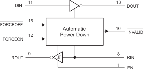
 Figure 8-1 Logic Diagram