JAJSKT6B January 2021 – July 2024 TMUX6219-Q1
PRODUCTION DATA
- 1
- 1 特長
- 2 アプリケーション
- 3 概要
- 4 Pin Configuration and Functions
-
5 Specifications
- 5.1 Absolute Maximum Ratings
- 5.2 ESD Ratings
- 5.3 Thermal Information
- 5.4 Recommended Operating Conditions
- 5.5 Source or Drain Continuous Current
- 5.6 ±15 V Dual Supply: Electrical Characteristics
- 5.7 ±15 V Dual Supply: Switching Characteristics
- 5.8 36 V Single Supply: Electrical Characteristics
- 5.9 36 V Single Supply: Switching Characteristics
- 5.10 12 V Single Supply: Electrical Characteristics
- 5.11 12 V Single Supply: Switching Characteristics
- 5.12 ±5 V Dual Supply: Electrical Characteristics
- 5.13 ±5 V Dual Supply: Switching Characteristics
- 5.14 Typical Characteristics
-
6 Parameter Measurement Information
- 6.1 On-Resistance
- 6.2 Off-Leakage Current
- 6.3 On-Leakage Current
- 6.4 Transition Time
- 6.5 tON(EN) and tOFF(EN)
- 6.6 Break-Before-Make
- 6.7 tON (VDD) Time
- 6.8 Propagation Delay
- 6.9 Charge Injection
- 6.10 Off Isolation
- 6.11 Crosstalk
- 6.12 Bandwidth
- 6.13 THD + Noise
- 6.14 Power Supply Rejection Ratio (PSRR)
- 7 Detailed Description
- 8 Application and Implementation
- 9 Device and Documentation Support
- 10Revision History
- 11Mechanical, Packaging, and Orderable Information
6.9 Charge Injection
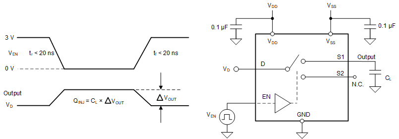
The TMUX6219-Q1 has a transmission-gate topology. Any mismatch in capacitance between the NMOS and PMOS transistors results in a charge injected into the drain or source during the falling or rising edge of the gate signal. The amount of charge injected into the source or drain of the device is known as charge injection, and is denoted by the symbol QC. Figure 6-9 shows the setup used to measure charge injection from source (Sx) to drain (D).
 Figure 6-9 Charge-Injection
Measurement Setup