JAJSKU0A December 2020 – June 2021 PCM1820 , PCM1821
PRODUCTION DATA
- 1 特長
- 2 アプリケーション
- 3 概要
- 4 Revision History
- 5 Device Comparison Table
- 6 Pin Configuration and Functions
- 7 Specifications
-
8 Detailed Description
- 8.1 Overview
- 8.2 Functional Block Diagram
- 8.3
Feature Description
- 8.3.1 Hardware Control
- 8.3.2 Audio Serial Interfaces
- 8.3.3 Phase-Locked Loop (PLL) and Clock Generation
- 8.3.4 Input Channel Configurations
- 8.3.5 Reference Voltage
- 8.3.6
Signal-Chain Processing
- 8.3.6.1 Digital High-Pass Filter
- 8.3.6.2
Configurable Digital Decimation Filters
- 8.3.6.2.1
Linear Phase Filters
- 8.3.6.2.1.1 Sampling Rate: 8 kHz or 7.35 kHz
- 8.3.6.2.1.2 Sampling Rate: 16 kHz or 14.7 kHz
- 8.3.6.2.1.3 Sampling Rate: 24 kHz or 22.05 kHz
- 8.3.6.2.1.4 Sampling Rate: 32 kHz or 29.4 kHz
- 8.3.6.2.1.5 Sampling Rate: 48 kHz or 44.1 kHz
- 8.3.6.2.1.6 Sampling Rate: 96 kHz or 88.2 kHz
- 8.3.6.2.1.7 Sampling Rate: 192 kHz or 176.4 kHz
- 8.3.6.2.2 Low-Latency Filters
- 8.3.6.2.1
Linear Phase Filters
- 8.3.7 Dynamic Range Enhancer (DRE)
- 8.4 Device Functional Modes
- 9 Application and Implementation
- 10Power Supply Recommendations
- 11Layout
- 12Device and Documentation Support
- 13Mechanical, Packaging, and Orderable Information
9.2.3 Application Curves
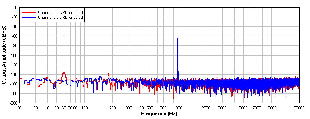
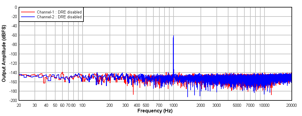
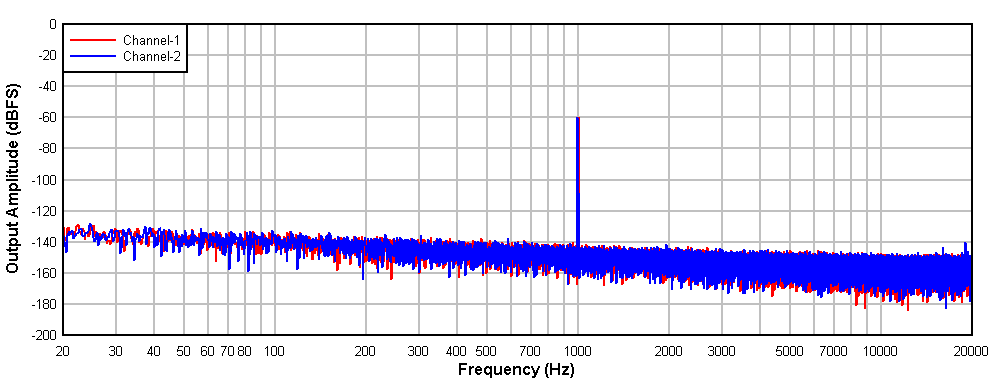
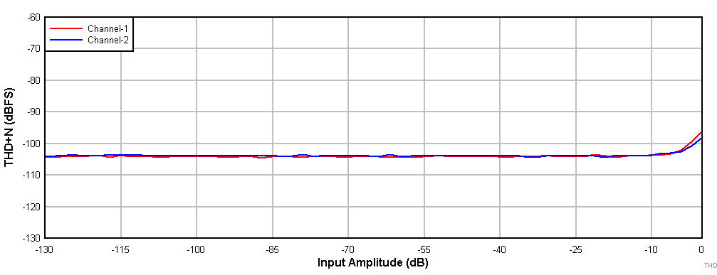
Measurements are done on the EVM by feeding the device analog input signal using audio precision and with a 3.3-V AVDD supply.
 Figure 9-2 PCM1820: FFT With a –60-dBr Input With DRE Enabled
 Figure 9-4 PCM1820: FFT With a –60-dBr Input With DRE Disabled
 Figure 9-6 PCM1821: FFT With a –60-dBr Input
 Figure 9-3 PCM1820: THD+N vs Input Amplitude With DRE Enabled
 Figure 9-5 PCM1820: THD+N vs Input Amplitude With DRE Disabled
 Figure 9-7 PCM1821: THD+N vs Input Amplitude