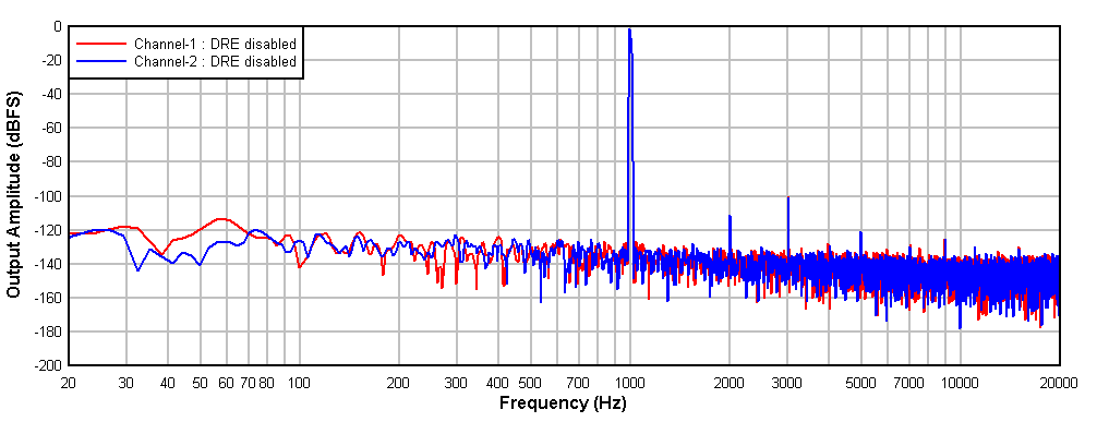
at TA = 25°C, AVDD = 3.3 V, IOVDD = 3.3
V, fIN = 1-kHz sinusoidal signal, fS = 48 kHz, 32-bit audio
data, BCLK = 256 × fS, TDM slave mode, PLL on, DRE_LVL = –36 dB, channel
gain = 0 dB, and linear phase decimation filter (unless otherwise noted); all
performance measurements are done with a 20-kHz, low-pass filter, and an A-weighted
filter
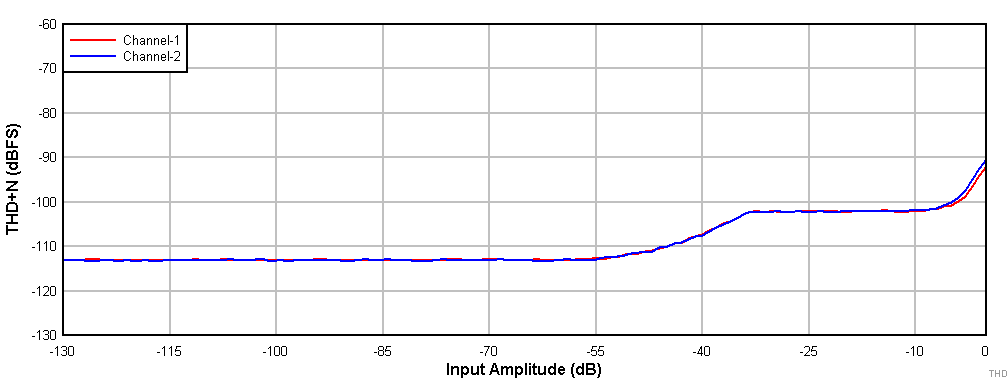
 Figure 7-4 THD+N
vs Input Amplitude With
DRE Enabled
 Figure 7-6 THD+N
vs Input Amplitude With
DRE Enabled
| Differential input with AVDD = 1.8 V and VREF = 1.375
V |
Figure 7-8 THD+N
vs Input Amplitude With
DRE Enabled Figure 7-10 THD+N
vs Input Frequency With a –60-dBr Input
 Figure 7-12 THD+N
vs Input Frequency With a –1-dBr Input
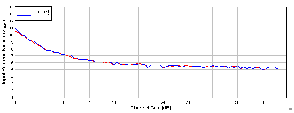
 Figure 7-14 Input-Referred Noise vs Channel Gain
 Figure 7-16 Frequency Response With a –30-dBr Input
 Figure 7-18 FFT
With Idle Input With DRE Enabled
 Figure 7-20 FFT
With a –60-dBr Input
With DRE Enabled
 Figure 7-22 FFT
With a –1-dBr Input With
DRE Enabled
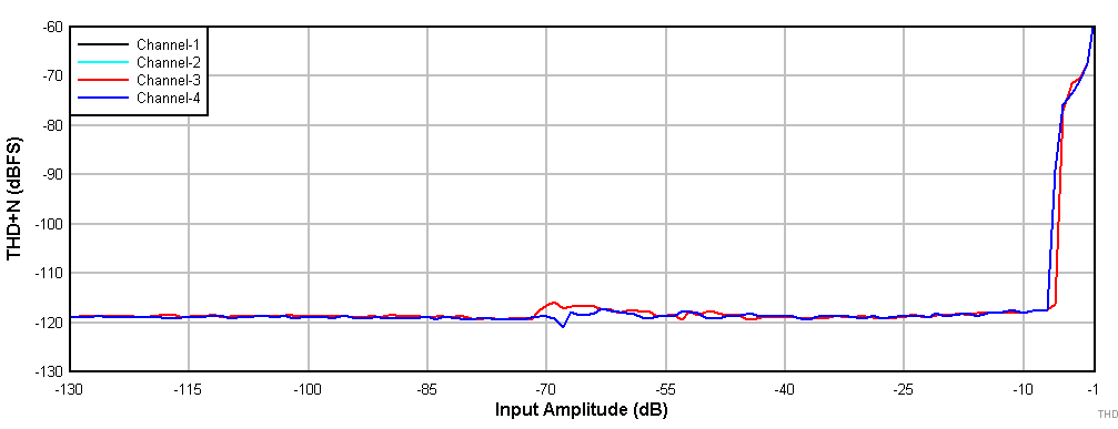
 Figure 7-24 PDM Input THD+N vs Input Amplitude
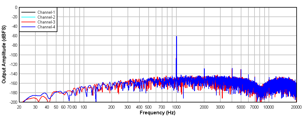
  Figure 7-26 PDM
Input FFT With a –60-dBr Input
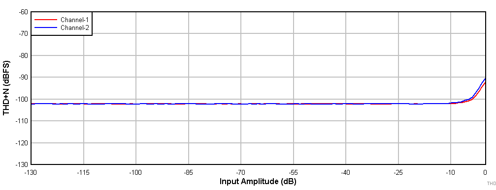
 Figure 7-5 THD+N
vs Input Amplitude With
DRE Disabled
 Figure 7-7 THD+N
vs Input Amplitude With
DRE Disabled
| Differential input with AVDD = 1.8 V and VREF = 1.375
V |
Figure 7-9 THD+N
vs Input Amplitude With
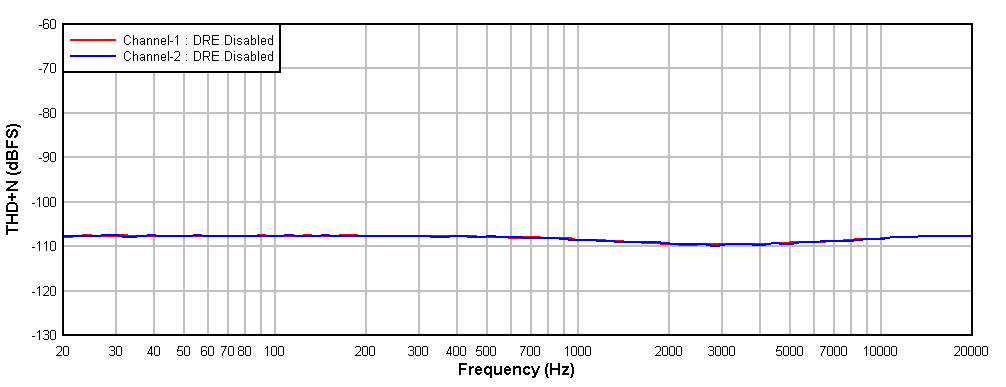
DRE Disabled Figure 7-11 THD+N vs Input Frequency With a –60-dBr
Input
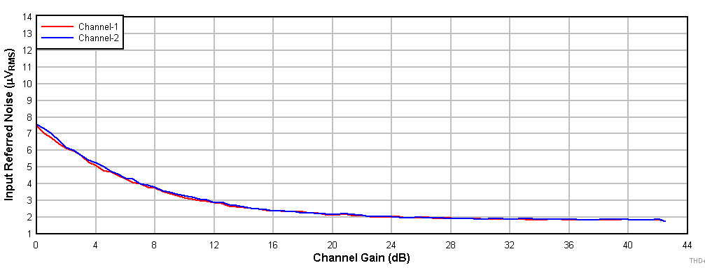
 Figure 7-13 Input-Referred Noise vs Channel Gain
 Figure 7-15 Frequency Response With a –12-dBr Input
 Figure 7-17 Power-Supply Rejection Ratio vs Ripple Frequency With 100-mVPP
Amplitude
 Figure 7-19 FFT
With Idle Input With DRE
Disabled
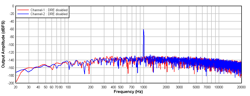
 Figure 7-21 FFT
With a –60-dBr Input
With DRE Disabled
 Figure 7-23 FFT
With a –1-dBr Input With
DRE Disabled
 Figure 7-25 PDM
Input THD+N vs Input Frequency With a
–20-dBr
Input Figure 7-27 PDM
Input Frequency Response With a
–20-dBr
Input

