JAJSL08H september   2009  – february 2021 BQ24040 , BQ24041 , BQ24045

PRODUCTION DATA  

  1.   1
  2. 特長
  3. アプリケーション
  4. 概要
  5. Revision History
  6. Device Comparison
  7. Pin Configuration and Functions
  8. Specifications
    1. 7.1 Absolute Maximum Ratings
    2. 7.2 ESD Ratings
    3. 7.3 Recommended Operating Conditions
    4. 7.4 Thermal Information
    5. 7.5 Electrical Characteristics
    6. 7.6 Timing Requirements
    7. 7.7 Typical Operational Characteristics (Protection Circuits Waveforms)
  9. Detailed Description
    1. 8.1 Overview
    2. 8.2 Functional Block Diagram
    3. 8.3 Feature Description
      1. 8.3.1 Power-Down or Undervoltage Lockout (UVLO)
      2. 8.3.2 Power-up
      3. 8.3.3 Sleep Mode
      4. 8.3.4 New Charge Cycle
      5. 8.3.5 Overvoltage-Protection (OVP) – Continuously Monitored
      6. 8.3.6 Power Good Indication ( PG)
      7. 8.3.7 CHG Terminal Indication
    4. 8.4 Device Functional Modes
      1. 8.4.1  CHG and PG LED Pull-up Source
      2. 8.4.2  Auto Start-up (BQ24041)
      3. 8.4.3  IN-DPM (VIN-DPM or IN-DPM)
      4. 8.4.4  OUT
      5. 8.4.5  ISET
      6. 8.4.6  PRE_TERM – Pre-Charge and Termination Programmable Threshold, BQ24040/5
      7. 8.4.7  ISET2
      8. 8.4.8  TS (BQ24040/5)
      9. 8.4.9  Termination and Timer Disable Mode (TTDM) - TS Terminal High
      10. 8.4.10 Timers, BQ24040 and BQ24045 only
      11. 8.4.11 Termination
      12. 8.4.12 Battery Detect Routine
      13. 8.4.13 Refresh Threshold
      14. 8.4.14 Starting a Charge on a Full Battery
  10. Application and Implementation
    1. 9.1 Application Information
    2. 9.2 Typical Applications
      1. 9.2.1 Typical Application: BQ24040 and BQ24045
        1. 9.2.1.1 Design Requirements
        2. 9.2.1.2 Detailed Design Procedure
          1. 9.2.1.2.1 Calculations
            1. 9.2.1.2.1.1 Program the Fast Charge Current, ISET:
            2. 9.2.1.2.1.2 Program the Termination Current Threshold, ITERM:
            3. 9.2.1.2.1.3 TS Function (BQ24040)
            4. 9.2.1.2.1.4 CHG and PG
          2. 9.2.1.2.2 Selecting In and Out Terminal Capacitors
        3. 9.2.1.3 Application Curves
      2. 9.2.2 Typical Application Circuit: BQ24041, with ASI and ASO
        1. 9.2.2.1 Design Requirements
        2. 9.2.2.2 Detailed Design Procedure
        3. 9.2.2.3 Application Curves
  11. 10Power Supply Recommendations
  12. 11Layout
    1. 11.1 Layout Guidelines
    2. 11.2 Layout Example
    3. 11.3 Thermal Considerations
      1. 11.3.1 Leakage Current Effects on Battery Capacity
  13. 12Device and Documentation Support
    1. 12.1 Device Support
      1. 12.1.1 サード・パーティ製品に関する免責事項
    2. 12.2 Documentation Support
      1. 12.2.1 Related Documentation
    3. 12.3 ドキュメントの更新通知を受け取る方法
    4. 12.4 サポート・リソース
    5. 12.5 Trademarks
    6. 12.6 静電気放電に関する注意事項
    7. 12.7 用語集
  14. 13Mechanical, Packaging, and Orderable Information

Application Curves

SETUP: BQ24040 typical applications schematic; VIN = 5V, VBAT = 3.6V (unless otherwise indicated)
GUID-1D47607F-0484-43B0-8878-0E62412ADB22-low.gif
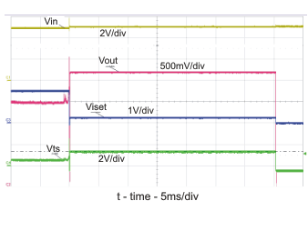
Figure 9-2 Power-up Timing
GUID-4FC91B31-FD30-4E21-8D31-1EFA5B3B6A12-low.gif
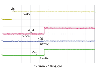
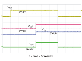
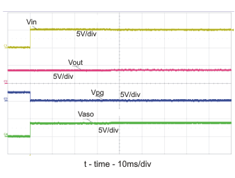
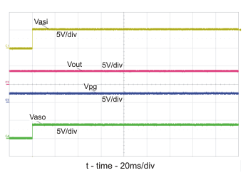
Figure 9-4 – ASI and OUT Power-up Timing – No Input  
GUID-829C231D-D7C9-4A4A-A2FE-B24EE7C4A9B1-low.gif
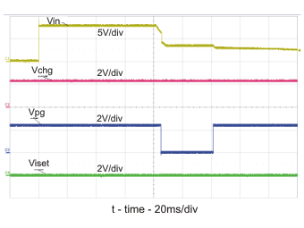
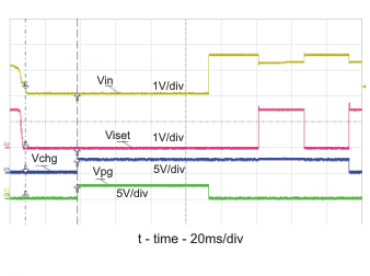
Figure 9-6 OVP 8V Adaptor - Hot Plug  
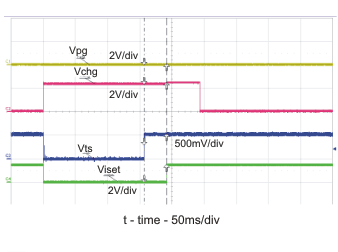
GUID-39FC496B-E1CE-4ECB-9ACD-59C9933CBB2E-low.gif
10kΩ resistor from TS to GND. 10kΩ is shorted to disable the IC
.
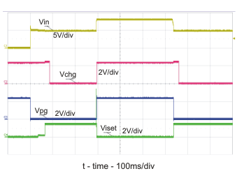
Figure 9-8 TS Enable and Disable  
GUID-72F6FB69-176E-4012-87C3-3F48751BB724-low.gif
Figure 9-10 Battery Removal – GND Removed 1st, 42 Ω Load  
GUID-F7A71E65-EE2F-49D5-9380-A937F0238E16-low.gif
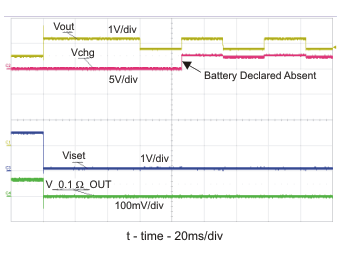
Continuous battery detection when not in TTDM
Figure 9-12 Battery Removal with fixed TS = 0.5V  
GUID-C289CC3B-F575-486C-BE24-0BF74C9E9C47-low.gif
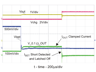
CH4: IOUT (1A/Div)
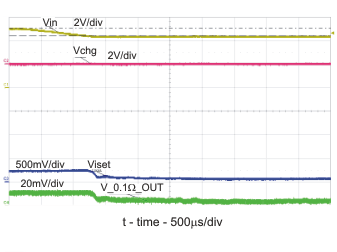
Figure 9-14 ISET Shorted During Normal Operation  
GUID-AEB369B8-46EA-4D97-8A55-B01BD144D874-low.gif
CH4: IOUT (0.2A/Div)
Figure 9-16 DPM – Adaptor Current Limits – Vin Regulated  
GUID-97A43896-8D02-4455-A712-DC9F3A6FCAE3-low.gif
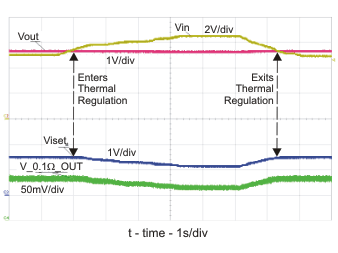
The IC temperature rises to 125°C and enters thermal regulation. Charge current is reduced to regulate the IC at 125°C. VIN is reduced, the IC temperature drops, the charge current returns to the programmed value
.
Figure 9-18 Thermal Reg. – Vin increases PWR/Iout Reduced
GUID-77BCAC66-511A-4C74-830F-1EF7987C1723-low.gif
Figure 9-3 Power-up Timing – No Battery or Load  
GUID-A09665E9-3899-4BA5-AD89-D4F0A53442F3-low.gif
Figure 9-5 ASI and delayed OUT Power-up Timing – No Input  
GUID-36F50CB4-F01A-4407-BB36-0355518E0A09-low.gif
Figure 9-7 OVP from Normal Power-up Operation – VIN 0V → 5V → 8V →5V  
GUID-A077ECA7-FCE0-497A-AFAB-216FD52F3771-low.gif
Fixed 10kΩ resistor, between TS and GND.
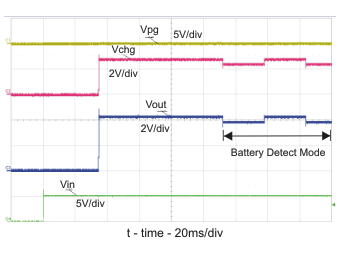
Figure 9-9 Hot Plug Source w/No Battery – Battery Detection  
GUID-D0F744A2-C2BA-42DE-B743-F11D5DC7E66A-low.gif
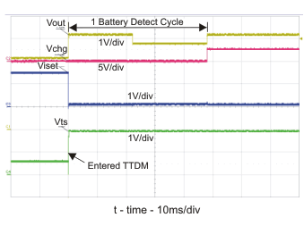
Figure 9-11 Battery Removal with OUT and TS Disconnect 1st, With 100 Ω Load  
GUID-E1BC5A90-580F-4A1D-A354-F555F9881D18-low.gif
CH4: IOUT (1A/Div)
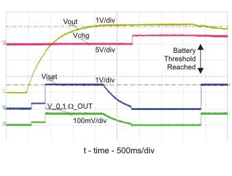
Battery voltage swept from 0V to 4.25V to 3.9V.
Figure 9-13 Battery Charge Profile  
GUID-EC441651-9CE0-42BF-99AC-223D7059A32D-low.gif
CH4: IOUT (0.2A/Div)
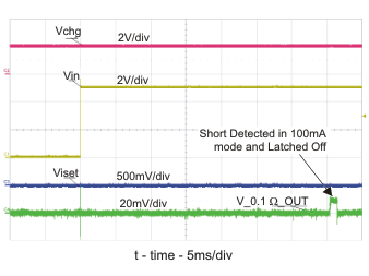
Figure 9-15 ISET Shorted Prior to USB Power-up  
GUID-32E24D7A-7CCA-4554-AFBD-BCBD648DA6BD-low.gif
Figure 9-17 DPM – USB Current Limits – Vin Regulated to 4.4V  
GUID-D12CF827-4CBA-4D04-98E4-69A14B6C2097-low.gif
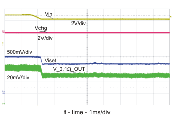
VIN swept from 5V to 3.9V to 5VVBAT = 4V
Figure 9-19 Entering and Exiting Sleep mode