JAJSLC9A
February 2021 – August 2021
TCA9416
PRODUCTION DATA
1
特長
2
アプリケーション
3
概要
4
Revision History
5
Pin Configuration and Functions
6
Specifications
6.1
Absolute Maximum Ratings
6.2
ESD Ratings
6.3
Recommended Operating Conditions
6.4
Thermal Information
6.5
Electrical Characteristics
6.6
Timing Requirements
6.7
Switching Characteristics
6.8
Typical Characteristics
7
Parameter Measurement Information
7.1
Voltage Waveforms
8
Detailed Description
8.1
Overview
8.2
Functional Block Diagram
8.3
Feature Description
8.3.1
Architecture
8.3.2
Enable and Disable
8.3.3
Pull up resistors on I/O Lines
8.4
Device Functional Modes
9
Application and Implementation
9.1
Application Information
9.2
Typical Application
9.2.1
Design Requirements
9.2.2
Detailed Design Procedure
9.2.2.1
Startup Considerations with Large Capacitive Load Mismatches
9.2.3
Application Curve
10
Power Supply Recommendations
11
Layout
11.1
Layout Guidelines
11.2
Layout Example
12
Device and Documentation Support
12.1
Receiving Notification of Documentation Updates
12.2
サポート・リソース
12.3
Trademarks
12.4
Electrostatic Discharge Caution
12.5
Glossary
7
Parameter Measurement Information
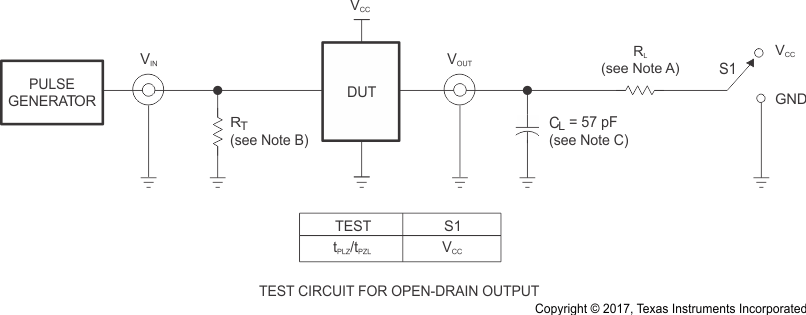
Figure 7-1
Load Circuit for Pulse Duration, Propagation Delay, Output Rise-Time and Fall-Time Measurement
R
L
= 1.35 kΩ
R
T
termination resistance should be equal to Z
OUT
of pulse generators.
C
L
includes probe and jig capacitance. C
L
= 50 pF when on the B-side.
All input pulses are supplied by generators having the following characteristics: PRR ≤ 10 MHz, Z
O
= 50 Ω, slew rate ≥ 1 V/ns.
t
PLZ
and t
PHZ
are the same as t
dis
.
t
PZL
and t
PZH
are the same as t
en
.
V
CCI
is the V
CC
associated with the input port.
V
CCO
is the V
CC
associated with the output port.