JAJSLC9A February   2021  – August 2021 TCA9416

PRODUCTION DATA  

  1. 特長
  2. アプリケーション
  3. 概要
  4. Revision History
  5. Pin Configuration and Functions
  6. Specifications
    1. 6.1 Absolute Maximum Ratings
    2. 6.2 ESD Ratings
    3. 6.3 Recommended Operating Conditions
    4. 6.4 Thermal Information
    5. 6.5 Electrical Characteristics
    6. 6.6 Timing Requirements
    7. 6.7 Switching Characteristics
    8. 6.8 Typical Characteristics
  7. Parameter Measurement Information
    1. 7.1 Voltage Waveforms
  8. Detailed Description
    1. 8.1 Overview
    2. 8.2 Functional Block Diagram
    3. 8.3 Feature Description
      1. 8.3.1 Architecture
      2. 8.3.2 Enable and Disable
      3. 8.3.3 Pull up resistors on I/O Lines
    4. 8.4 Device Functional Modes
  9. Application and Implementation
    1. 9.1 Application Information
    2. 9.2 Typical Application
      1. 9.2.1 Design Requirements
      2. 9.2.2 Detailed Design Procedure
        1. 9.2.2.1 Startup Considerations with Large Capacitive Load Mismatches
      3. 9.2.3 Application Curve
  10. 10Power Supply Recommendations
  11. 11Layout
    1. 11.1 Layout Guidelines
    2. 11.2 Layout Example
  12. 12Device and Documentation Support
    1. 12.1 Receiving Notification of Documentation Updates
    2. 12.2 サポート・リソース
    3. 12.3 Trademarks
    4. 12.4 Electrostatic Discharge Caution
    5. 12.5 Glossary

Voltage Waveforms

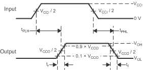
GUID-FD5E844C-B925-4216-A970-6AC0BB661055-low.gifFigure 7-2 Propagation Delay Times

  1. CL includes probe and jig capacitance.
  2. Waveform 1 in Figure 7-3 is for an output with internal such that the output is high, except when OE is high (see Figure 7-1). Waveform 2 in Figure 7-3 is for an output with conditions such that the output is low, except when OE is high.
  3. All input pulses are supplied by generators having the following characteristics: PRR ≤ 10 MHz, ZO = 50 Ω, dv/dt ≥ 1 V/ns.
  4. The outputs are measured one at a time, with one transition per measurement.
  5. tPLZ and tPHZ are the same as tdis.
  6. tPZL and tPZH are the same as ten.
  7. tPLH and tPHL are the same as tpd.
  8. VCCI is the VCC associated with the input port.
  9. VCCO is the VCC associated with the output port.
Figure 7-3 Enable and Disable Times