JAJSLE0B March 2021 – November 2022 TMUX7411F , TMUX7412F , TMUX7413F
PRODMIX
- 1 特長
- 2 アプリケーション
- 3 概要
- 4 Revision History
- 5 Device Comparison Table
- 6 Pin Configuration and Functions
-
7 Specifications
- 7.1 Absolute Maximum Ratings
- 7.2 ESD Ratings
- 7.3 Thermal Information
- 7.4 Recommended Operating Conditions
- 7.5 Electrical Characteristics: Global
- 7.6 ±15 V Dual Supply: Electrical Characteristics
- 7.7 ±20 V Dual Supply: Electrical Characteristics
- 7.8 12 V Single Supply: Electrical Characteristics
- 7.9 36 V Single Supply: Electrical Characteristics
- 7.10 Typical Characteristics
-
8 Parameter Measurement Information
- 8.1 On-Resistance
- 8.2 Turn-On and Turn-Off Time
- 8.3 Off-Leakage Current
- 8.4 On-Leakage Current
- 8.5 Input and Output Leakage Current Under Overvoltage Fault
- 8.6 Fault Response Time
- 8.7 Fault Recovery Time
- 8.8 Fault Flag Response Time
- 8.9 Fault Flag Recovery Time
- 8.10 Charge Injection
- 8.11 Off Isolation
- 8.12 Inter-Channel Crosstalk
- 8.13 Bandwidth
- 8.14 THD + Noise
- 9 Detailed Description
- 10Application and Implementation
- 11Power Supply Recommendations
- 12Layout
- 13Device and Documentation Support
- 14Mechanical, Packaging, and Orderable Information
8.5 Input and Output Leakage Current Under Overvoltage Fault
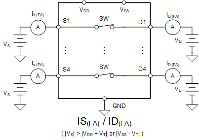
If any of the source pin voltage goes above the supplies (VDD or VSS) by one threshold voltage (VT), then the overvoltage protection feature of the TMUX7411F, TMUX7412F, and TMUX7413F is triggered to turn off the switch under fault, keeping the fault channel in a high-impedance state. IS(FA) and ID(FA) denotes the input and output leakage current under overvoltage fault conditions, respectively. When the overvoltage fault occurs, the supply (or supplies) can either be in normal operating condition (Figure 8-5) or abnormal operating condition (Figure 8-6). During abnormal operating condition, the supply (or supplies) can either be unpowered (VDD= VSS = 0 V) or floating (VDD= VSS = no connection), and remains within the leakage performance specifications.
 Figure 8-5 Measurement Setup for Input
and Output Leakage Current under Overvoltage Fault with Normal Supplies
 Figure 8-6 Measurement Setup for Input
and Output Leakage Current under Overvoltage Fault with Unpowered or Floating
Supplies