JAJSLN2 November 2021 TPS7H1210-SEP
PRODUCTION DATA
- 1 特長
- 2 アプリケーション
- 3 概要
- 4 Revision History
- 5 Pin Configuration and Functions
- 6 Specifications
- 7 Detailed Description
- 8 Application and Implementation
- 9 Power Supply Recommendations
- 10Layout
- 11Device and Documentation Support
- 12Mechanical, Packaging, and Orderable Information
5 Pin Configuration and Functions
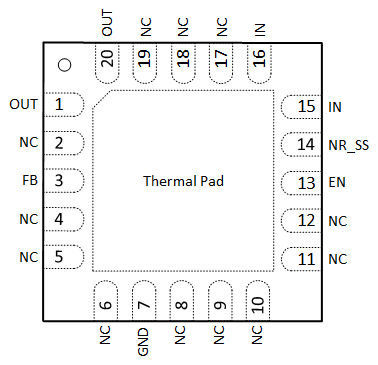
 Figure 5-1 RGW Package,20-Pin VQFN(Top View)
Table 5-1 Pin Functions
| PIN | I/O(1) | DESCRIPTION | |
|---|---|---|---|
| NAME | NO. | ||
| EN | 13 | I | Enable. This dual-polarity pin turns the regulator on when |VEN| ≥ 2 V. The EN pin can be connected to IN if not used. If VEN is negative polarity, then keep |VEN| ≤ |VIN|. |
| FB | 3 | I | Feedback. This pin is the input to the control-loop error amplifier. It is used to set the output voltage of the device and is normally equal to VREF (–1.182 V, typical) during operation. |
| GND | 7 | — | Ground. |
| IN | 15, 16 | I | Input supply. It is recommended to connect a 10-µF capacitor from IN to GND (as close to the device as possible). |
| NC | 2, 4–6, 8–12, 17–19 | — | No connect. This pin is not internally connected. It is recommended to connect these pins to GND to prevent charge buildup; however, these pins can also be left open or tied to any voltage between GND and VIN. |
| NR_SS | 14 | — | Noise reduction and soft start. A capacitor connected from this pin to GND controls the soft-start function and allows RMS noise to be reduced to very low levels. TI recommends connecting a 100-nF capacitor from NR_SS to GND (as close to the device as possible) to filter the noise generated by the internal band gap and maximize AC performance. |
| OUT | 1, 20 | O | Output of the regulator. A capacitor greater than or equal to 10 µF must be tied from this pin to ground to ensure stability. TI recommends connecting a 47-µF ceramic capacitor from OUT to GND (as close to the device as possible) to maximize AC performance. |
| Thermal Pad |
— | — | Connect the thermal pad to a large-area ground plane. The thermal pad is not internally grounded and it must be externally tied to GND for proper operation. |
(1) I = Input, O = Output, — =
Other