JAJSM94B June   2021  – June 2022 DAC12DL3200

PRODUCTION DATA  

  1. 特長
  2. アプリケーション
  3. 概要
  4. Revision History
  5. Pin Configuration and Functions
  6. Specifications
    1. 6.1  Absolute Maximum Ratings
    2. 6.2  ESD Ratings
    3. 6.3  Recommended Operating Conditions
    4. 6.4  Thermal Information
    5. 6.5  Electrical Characteristics - DC Specifications
    6. 6.6  Electrical Characteristics - Power Consumption
    7. 6.7  Electrical Characteristics - AC Specifications
    8. 6.8  Timing Requirements
    9. 6.9  Switching Characteristics
    10. 6.10 Typical Characteristics
  7. Detailed Description
    1. 7.1 Overview
    2. 7.2 Functional Block Diagram
    3. 7.3 Feature Description
      1. 7.3.1 DAC Output Modes
        1. 7.3.1.1 NRZ Mode
        2. 7.3.1.2 RTZ Mode
        3. 7.3.1.3 RF Mode
        4. 7.3.1.4 2xRF Mode
      2. 7.3.2 DAC Output Interface
        1. 7.3.2.1 DAC Output Structure
        2. 7.3.2.2 Full-scale Current Adjustment
        3. 7.3.2.3 Example Analog Output Interfaces
      3. 7.3.3 LVDS Interface
        1. 7.3.3.1 MODE0: Two LVDS banks per channel
        2. 7.3.3.2 MODE1: One LVDS bank per channel
        3. 7.3.3.3 MODE2: Four LVDS banks, single channel mode
        4. 7.3.3.4 LVDS Interface Input Strobe
        5. 7.3.3.5 FIFO Operation
          1. 7.3.3.5.1 Using FIFO Delay Readback Values
          2. 7.3.3.5.2 FIFO Delay Handling
          3. 7.3.3.5.3 FIFO Delay and NCO Operation
          4. 7.3.3.5.4 FIFO Over/Under Flow Alarming
      4. 7.3.4 Multi-Device Synchronization (SYSREF+/-)
        1. 7.3.4.1 DACCLK Domain Synchronization
        2. 7.3.4.2 SYSREF Position Detector and Sampling Position Selection (SYSREF Windowing)
      5. 7.3.5 Alarms
    4. 7.4 Device Functional Modes
      1. 7.4.1 Direct Digital Synthesis (DDS) Mode
        1. 7.4.1.1 NCO Gain Scaling
        2. 7.4.1.2 NCO Phase Continuous Operation
        3. 7.4.1.3 Trigger Clock
    5. 7.5 Programming
      1. 7.5.1 Using the Serial Interface
        1. 7.5.1.1 SCS
        2. 7.5.1.2 SCLK
        3. 7.5.1.3 SDI
        4. 7.5.1.4 SDO
        5. 7.5.1.5 Serial Interface Operation
        6. 7.5.1.6 Streaming Mode
      2. 7.5.2 SPI Register Map
  8. Application and Implementation
    1. 8.1 Application Information
      1. 8.1.1 Startup Procedure with LVDS Input
      2. 8.1.2 Startup Procedure With NCO Operation
      3. 8.1.3 Interface Test Pattern and Timing Verification
    2. 8.2 Typical Application
      1. 8.2.1 Design Requirements
      2. 8.2.2 Detailed Design Procedure
      3. 8.2.3 Application Curves
    3. 8.3 Power Supply Recommendations
      1. 8.3.1 Power Up and Down Sequence
    4. 8.4 Layout
      1. 8.4.1 Layout Guidelines
      2. 8.4.2 Layout Example
  9. Device and Documentation Support
    1. 9.1 Receiving Notification of Documentation Updates
    2. 9.2 サポート・リソース
    3. 9.3 Trademarks
    4. 9.4 Electrostatic Discharge Caution
    5. 9.5 Glossary
  10. 10Mechanical, Packaging, and Orderable Information
FIFO Over/Under Flow Alarming

Each of the capture flops on the read side of the FIFO is actually constructed of 3 flops (see Figure 7-20). This allows detection of close timing violations that could corrupt the data flop and is used for detecting under and overflow alarms. This will only detect slow drifts. It will not detect sudden jumps in the operation that might jump over the alarm detection. This will also only detect alarms if the violation occurs when the data is changing. Constant input data will not produce alarms.
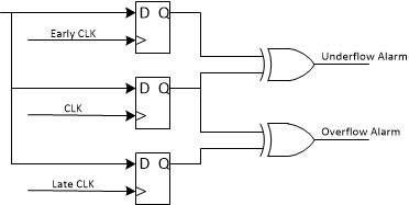
GUID-20200917-CA0I-0PLR-P1VB-RCXVFW3HRWK3-low.gif Figure 7-20 Datapath Showing FIFO Over/Under Flow Alarming