JAJSMM4H July   2001  – September 2024 PCF8574A

PRODUCTION DATA  

  1.   1
  2. 特長
  3. アプリケーション
  4. 概要
  5. Pin Configuration and Functions
  6. Specifications
    1. 5.1 Absolute Maximum Ratings
    2. 5.2 ESD Ratings
    3. 5.3 Recommended Operating Conditions
    4. 5.4 Thermal Information
    5. 5.5 Electrical Characteristics
    6. 5.6 I2C Interface Timing Requirements
    7. 5.7 Switching Characteristics
    8. 5.8 Typical Characteristics
  7. Parameter Measurement Information
  8. Detailed Description
    1. 7.1 Overview
    2. 7.2 Functional Block Diagram
      1. 7.2.1 Simplified Block Diagram of Device
      2. 7.2.2 Simplified Schematic Diagram of Each P-Port Input/Output
    3. 7.3 Feature Description
      1. 7.3.1 I2C Interface
      2. 7.3.2 Interface Definition
      3. 7.3.3 Address Reference
    4. 7.4 Device Functional Modes
  9. Application Information Disclaimer
    1. 8.1 Application Information
    2. 8.2 Typical Application
      1. 8.2.1 Design Requirements
        1. 8.2.1.1 Minimizing ICC When I/Os Control LEDs
      2. 8.2.2 Detailed Design Procedure
      3. 8.2.3 Application Curves
    3. 8.3 Power Supply Recommendations
      1. 8.3.1 Power-On Reset Requirements
    4. 8.4 Layout
      1. 8.4.1 Layout Guidelines
      2. 8.4.2 Layout Example
  10. Device and Documentation Support
    1. 9.1 Documentation Support
      1. 9.1.1 Glossary
    2. 9.2 Receiving Notification of Documentation Updates
    3. 9.3 サポート・リソース
    4. 9.4 Trademarks
    5. 9.5 静電気放電に関する注意事項
    6. 9.6 用語集
  11. 10Revision History
  12. 11Mechanical, Packaging, and Orderable Information

Device Functional Modes

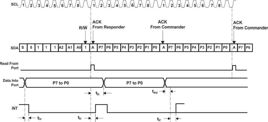
Figure 7-1 and Figure 7-2 show the address and timing diagrams for the write and read modes, respectively.
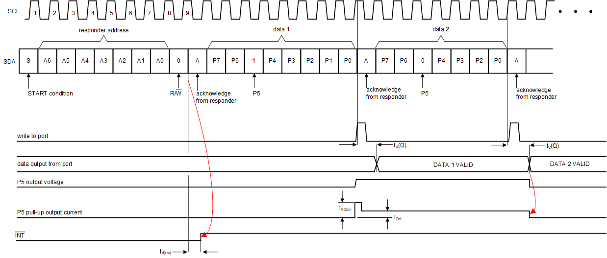
PCF8574A Write Mode (Output)Figure 7-1 Write Mode (Output)
PCF8574A Read Mode (Input)
A low-to-high transition of SDA while SCL is high is defined as the stop condition (P). The transfer of data can be stopped at any moment bya stop condition. When this occurs, data present at the latest ACK phase is valid (output mode). Input data is lost.
Figure 7-2 Read Mode (Input)