JAJSMP8C May 2023 – June 2024 OPT4001-Q1
PRODUCTION DATA
- 1
- 1 特長
- 2 アプリケーション
- 3 概要
- 4 Pin Configuration and Functions
- 5 Specifications
- 6 Detailed Description
- 7 Register Maps
-
8 Application and Implementation
- 8.1 Application Information
- 8.2 Typical Application
- 8.3 Best Design Practices
- 8.4 Power Supply Recommendations
- 8.5 Layout
- 9 デバイスおよびドキュメントのサポート
- 10Revision History
- 11Mechanical, Packaging, and Orderable Information
8.5.1 Layout Guidelines
 Figure 8-9 Placement Side View of
Packages
Figure 8-9 Placement Side View of
PackagesIn the case of the USON package variant of the device, since the lighting sensitive area and the device pins are on opposite sides of each other, a conventional placement on the PCB provides good light collection. In the case of the PicoStar™ variant of the device, since the light sensitive area and the device pins are on the same side, a special arrangement as shown in Figure 8-9 is required to achieve good light collection. Typically, a thin flexible PCB with a hole or a cutout centered around the optical area is required for wide-angle light collection for the PicoStar™ variant. A regular PCB can be used but the amount of light collected and the field of view of light collection are not very good and generally not recommended. The cut out for the light collection can be of any shape with a large enough opening to let ample light fall on the light sensitive area. Figure 8-15 and Figure 8-16 show examples of two shapes which help maximize light collection. A circular cut out as large as manufacturing allows is acceptable but can restrict the field of view and reduce the light collection. Tools and documentation are available on TI's product folder to estimate the field of view based on the hole size.
TI highly recommends placing the decoupling capacitor close to the device, but remember that optically reflective surfaces of components also affect the performance of the design. Consider the three-dimensional geometry of all components and structures around the sensor to prevent unexpected results from secondary optical reflections. Placing capacitors and components at a distance of at least twice the height of the component is usually sufficient. The best optical layout is to place all close components on the opposite side of the PCB from the OPT4001-Q1. However, this approach is not practical for the constraints of every design.
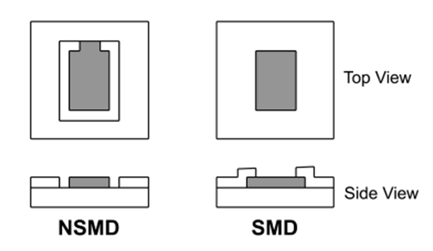
The device layout is also critical for good SMT assembly. Two types of land pattern pads can be used for this package: solder mask defined pads (SMD) and non-solder mask defined pads (NSMD). SMD pads have a solder mask opening that is smaller than the metal pads, whereas, NSMD has a solder mask opening that is larger than the metal pad. Figure 8-10 illustrates these types of landing-pattern pads. SMD pads are preferred because these pads provide a more accurate soldering-pad dimension with the trace connections. For further discussion of SMT and PCB recommendations, see the Soldering and Handling Recommendations (USON Variant) section.
 Figure 8-10 Solder Mask Defined Pad (SMD) and Non-Solder Mask Defined Pad (NSMD)