JAJSMX1B September 2021 – March 2022 LM74720-Q1
PRODUCTION DATA
- 1 特長
- 2 アプリケーション
- 3 概要
- 4 Revision History
- 5 Pin Configuration and Functions
- 6 Specifications
- 7 Parameter Measurement Information
- 8 Detailed Description
-
9 Application and Implementation
- 9.1 Application Information
- 9.2
Typical 12-V Reverse Battery Protection Application
- 9.2.1 Design Requirements for 12-V Battery Protection
- 9.2.2 Automotive Reverse Battery Protection
- 9.2.3
Detailed Design Procedure
- 9.2.3.1 Design Considerations
- 9.2.3.2 Boost Converter Components (C2, C3, L1)
- 9.2.3.3 Input and Output Capacitance
- 9.2.3.4 Hold-Up Capacitance
- 9.2.3.5 Overvoltage Protection and Battery Monitor
- 9.2.3.6 MOSFET Selection: Blocking MOSFET Q1
- 9.2.3.7 MOSFET Selection: Load Disconnect MOSFET Q2
- 9.2.3.8 TVS Selection
- 9.2.4 Application Curves
- 9.3 Do's and Don'ts
- 10Power Supply Recommendations
- 11Layout
- 12Device and Documentation Support
- 13Mechanical, Packaging, and Orderable Information
9.2.2.2 AC Super Imposed Input Rectification: ISO 16750-2 and LV124 E-06
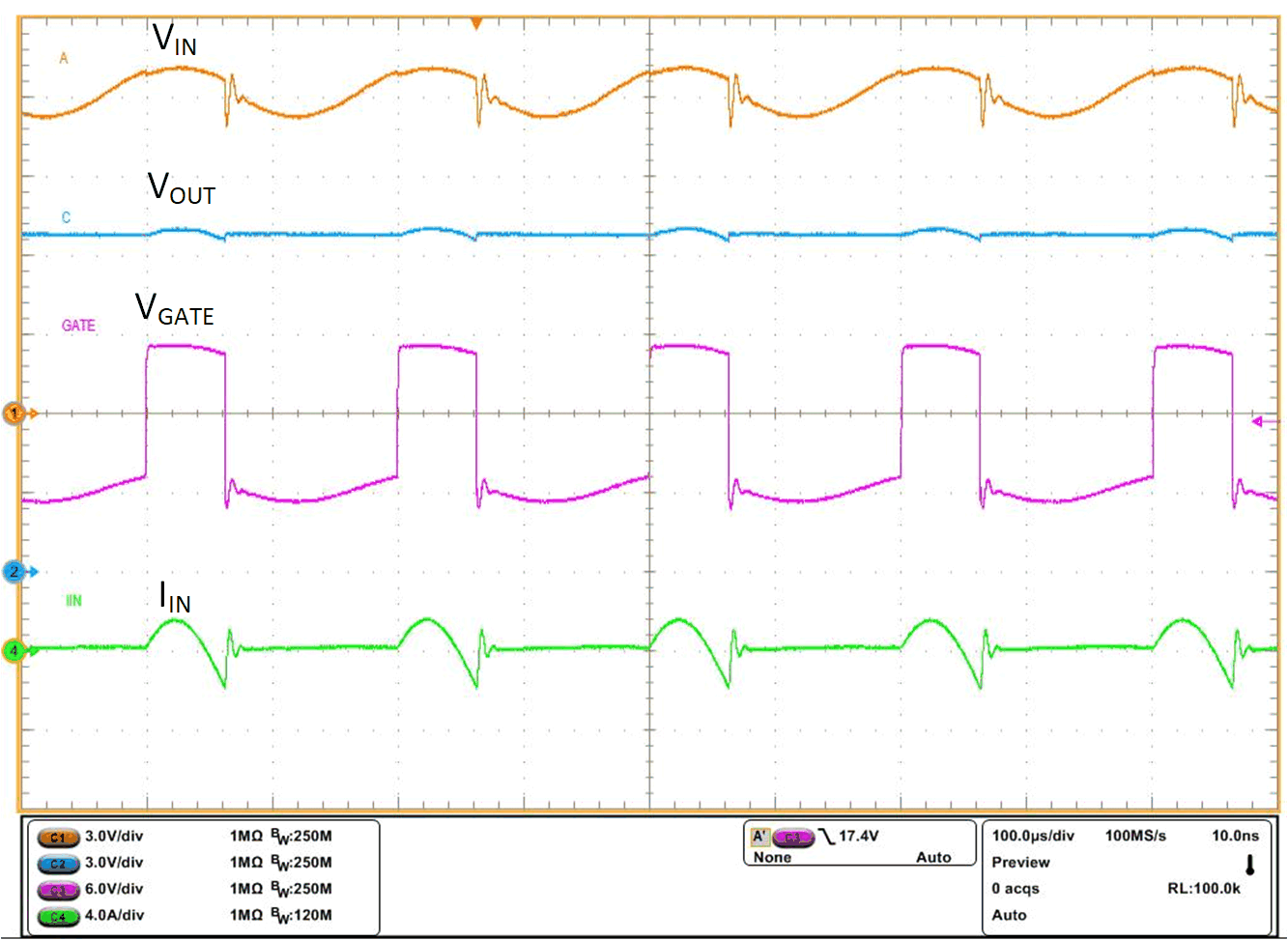
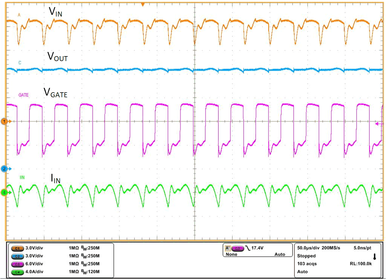
All electronic modules are tested for proper operation with superimposed AC ripple on the DC battery voltage. AC super imposed test specified in ISO 16750-2 and LV124 E-06 requires AC ripple of 2-V peak-peak on a 13.5-V DC battery voltage, swept from 15 Hz to 30 kHz. LM74720-Q1 rectifies the AC superimposed voltage by turning the MOSFET Q1 OFF quickly to cut off reverse current and turning the MOSFET Q1 ON quickly during forward conduction. Active rectification of 2-V peak-peak 5-kHz AC input by LM74720-Q1 is shown in Figure 9-3. Fast turn-OFF and quick turn-ON of the MOSFET reduces power dissipation in the MOSFET Q1 and active rectification reduces power dissipation in the output hold-up capacitor's ESR by half. Active rectification of 2-V peak-peak 30-kHz AC input is shown in Figure 9-4.
 Figure 9-3 AC Super Imposed Test – 2-V Peak-Peak 5 kHz
 Figure 9-4 AC Super Imposed Test – 2-V Peak-Peak 30 kHz