JAJSN29B october 2021 – march 2023 TMUX8211 , TMUX8212 , TMUX8213
PRODUCTION DATA
- 1 特長
- 2 アプリケーション
- 3 概要
- 4 Revision History
- 5 Device Comparison Table
- 6 Pin Configuration and Functions
-
7 Specifications
- 7.1 Absolute Maximum Ratings: TMUX821x Devices
- 7.2 ESD Ratings
- 7.3 Recommended Operating Conditions: TMUX821x Devices
- 7.4 ソースまたはドレイン連続電流
- 7.5 ドレイン・パルス電流のソース
- 7.6 Thermal Information
- 7.7 Electrical Characteristics (Global): TMUX821x Devices
- 7.8 Electrical Characteristics (±15-V Dual Supply)
- 7.9 Electrical Characteristics (±36-V Dual Supply)
- 7.10 Electrical Characteristics (±50-V Dual Supply)
- 7.11 Electrical Characteristics (72-V Single Supply)
- 7.12 Electrical Characteristics (100-V Single Supply)
- 7.13 Switching Characteristics: TMUX821x Devices
- 7.14 Typical Characteristics
- 8 Parameter Measurement Information
- 9 Detailed Description
- 10Application and Implementation
- 11Power Supply Recommendations
- 12Layout
- 13Device and Documentation Support
- 14Mechanical, Packaging, and Orderable Information
8.9 THD + Noise
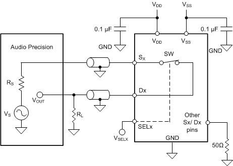
The total harmonic distortion (THD) of a signal is a measurement of the harmonic distortion, and is defined as the ratio of the sum of the powers of all harmonic components to the power of the fundamental frequency at the multiplexer output. The On-Resistance of the device varies with the amplitude of the input signal and results in distortion when the drain pin is connected to a low-impedance load. Total harmonic distortion plus noise is denoted as THD+N. Figure 8-9 shows the setup used to measure THD+N of the devices.
 Figure 8-9 THD+N Measurement
Setup