JAJSNA3 September   2024 TUSB1064-Q1

PRODUCTION DATA  

  1.   1
  2. 特長
  3. アプリケーション
  4. 概要
  5. Pin Configuration and Functions
  6. Specifications
    1. 5.1 Absolute Maximum Ratings
    2. 5.2 ESD Ratings
    3. 5.3 Recommended Operating Conditions
    4. 5.4 Thermal Information
    5. 5.5 Electrical Characteristics
    6. 5.6 Timing Requirements
    7. 5.7 Switching Characteristics
    8. 5.8 Typical Characteristics
  7. Parameter Measurement Information
  8. Detailed Description
    1. 7.1 Overview
    2. 7.2 Functional Block Diagram
    3. 7.3 Feature Description
      1. 7.3.1 USB 3.2
      2. 7.3.2 DisplayPort
      3. 7.3.3 4-Level Inputs
      4. 7.3.4 Receiver Linear Equalization
    4. 7.4 Device Functional Modes
      1. 7.4.1 Device Configuration in GPIO Mode
      2. 7.4.2 Device Configuration In I2C Mode
      3. 7.4.3 DisplayPort Mode
      4. 7.4.4 Linear EQ Configuration
      5. 7.4.5 USB3 Modes
      6. 7.4.6 Operation Timing – Power Up
    5. 7.5 Programming
      1. 7.5.1 TUSB1064-Q1 I2C Target Behavior
  9. Application and Implementation
    1. 8.1 Application Information
    2. 8.2 Typical Application
      1. 8.2.1 Design Requirements
      2. 8.2.2 Detailed Design Procedure
        1. 8.2.2.1 ESD Protection
        2. 8.2.2.2 Support for DisplayPort UFP_D Pin Assignment E
      3. 8.2.3 Application Curve
    3. 8.3 System Examples
      1. 8.3.1 USB 3.1 Only
      2. 8.3.2 USB 3.1 and 2 Lanes of DisplayPort
      3. 8.3.3 DisplayPort Only
    4. 8.4 Power Supply Recommendations
    5. 8.5 Layout
      1. 8.5.1 Layout Guidelines
      2. 8.5.2 Layout Example
  10. Register Maps
    1. 9.1 General Register (address = 0x0A) [reset = 00000001]
    2. 9.2 DisplayPort Control/Status Registers (address = 0x10) [reset = 00000000]
    3. 9.3 DisplayPort Control/Status Registers (address = 0x11) [reset = 00000000]
    4. 9.4 DisplayPort Control/Status Registers (address = 0x12) [reset = 00000000]
    5. 9.5 DisplayPort Control/Status Registers (address = 0x13) [reset = 00000000]
    6. 9.6 USB3.1 Control/Status Registers (address = 0x20) [reset = 00000000]
    7. 9.7 USB3.1 Control/Status Registers (address = 0x21) [reset = 00000000]
    8. 9.8 USB3.1 Control/Status Registers (address = 0x22) [reset = 00000000]
  11. 10Device and Documentation Support
    1. 10.1 ドキュメントの更新通知を受け取る方法
    2. 10.2 サポート・リソース
    3. 10.3 Trademarks
    4. 10.4 静電気放電に関する注意事項
    5. 10.5 用語集
  12. 11Revision History
  13. 12Mechanical, Packaging, and Orderable Information

USB 3.1 Only

The TUSB1064-Q1 is in USB3.1 only when the CTL1 pin is low and CTL0 pin is high.
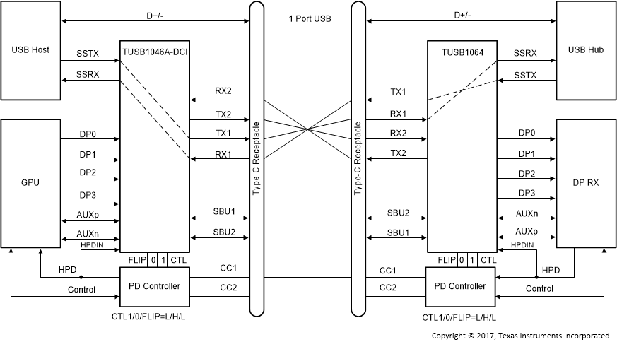
TUSB1064-Q1 USB3.1
                    Only – No Flip (CTL1 = L, CTL0 = H, FLIP = L) Figure 8-6 USB3.1 Only – No Flip (CTL1 = L, CTL0 = H, FLIP = L)
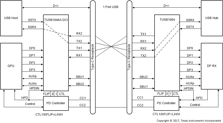
TUSB1064-Q1 USB3.1
                    Only – With Flip (CTL1 = L, CTL0 = H, FLIP = H) Figure 8-7 USB3.1 Only – With Flip (CTL1 = L, CTL0 = H, FLIP = H)