JAJSNB2D November 2021 – September 2024 AWR2944
PRODUCTION DATA
- 1
- 1 特長
- 2 アプリケーション
- 3 概要
- 4 Device Comparison
- 5 Pin Configurations and Functions
-
6 Specifications
- 6.1 Absolute Maximum Ratings
- 6.2 ESD Ratings
- 6.3 Power-On Hours (POH)
- 6.4 Recommended Operating Conditions
- 6.5 VPP Specifications for One-Time Programmable (OTP) eFuses
- 6.6 Power Supply Specifications
- 6.7 Power Consumption Summary
- 6.8 RF Specifications
- 6.9 Thermal Resistance Characteristics
- 6.10 Power Supply Sequencing and Reset Timing
- 6.11 Input Clocks and Oscillators
- 6.12
Peripheral Information
- 6.12.1
QSPI Flash Memory Peripheral
- 6.12.1.1 QSPI Timing Conditions
- 6.12.1.2 QSPI Timing Requirements #GUID-CD30070D-F132-4A2C-92CD-5AA96AE70B94/GUID-97D19708-D87E-443B-9ADF-1760CFEF6F4C #GUID-CD30070D-F132-4A2C-92CD-5AA96AE70B94/GUID-0A61EEC9-2B95-4C27-B219-18D27C8F9430
- 6.12.1.3 QSPI Switching Characteristics #GUID-20B35D26-AFE6-451C-B9E9-B3F2FA08097C/T4362547-64 #GUID-20B35D26-AFE6-451C-B9E9-B3F2FA08097C/T4362547-65
- 6.12.2
Multibuffered / Standard Serial Peripheral Interface (MibSPI)
- 6.12.2.1 MibSPI Peripheral Description
- 6.12.2.2
MibSPI Transmit and Receive RAM Organization
- 6.12.2.2.1 SPI Timing Conditions
- 6.12.2.2.2 SPI Controller Mode Switching Parameters (CLOCK PHASE = 0, SPICLK = output, SPISIMO = output, and SPISOMI = input) #GUID-20BA2ACF-4FC2-43F6-960F-1A4CA56E65A6/T4362547-236 #GUID-20BA2ACF-4FC2-43F6-960F-1A4CA56E65A6/T4362547-237 #GUID-20BA2ACF-4FC2-43F6-960F-1A4CA56E65A6/T4362547-238
- 6.12.2.2.3 SPI Controller Mode Switching Parameters (CLOCK PHASE = 1, SPICLK = output, SPISIMO = output, and SPISOMI = input) #GUID-517E5284-3345-461F-B07F-EB95741B1272/T4362547-244 #GUID-517E5284-3345-461F-B07F-EB95741B1272/T4362547-245 #GUID-517E5284-3345-461F-B07F-EB95741B1272/T4362547-246
- 6.12.2.3 SPI Peripheral Mode I/O Timings
- 6.12.3
Ethernet Switch (RGMII/RMII/MII)
Peripheral
- 6.12.3.1 RGMII Timing Conditions
- 6.12.3.2 RGMII Transmit Clock Switching Characteristics
- 6.12.3.3 RGMII Transmit Data and Control Switching Characteristics
- 6.12.3.4 RGMII Receive Clock Timing Requirements
- 6.12.3.5 RGMII Receive Data and Control Timing Requirements
- 6.12.3.6 RMII Transmit Clock Switching Characteristics
- 6.12.3.7 RMII Transmit Data and Control Switching Characteristics
- 6.12.3.8 RMII Receive Clock Timing Requirements
- 6.12.3.9 RMII Receive Data and Control Timing Requirements
- 6.12.3.10 MII Transmit Switching Characteristics
- 6.12.3.11 MII Receive Clock Timing Requirements
- 6.12.3.12 MII Receive Timing Requirements
- 6.12.3.13 MII Transmit Clock Timing Requirements
- 6.12.3.14 MDIO Interface Timings
- 6.12.4 LVDS/Aurora Instrumentation and Measurement Peripheral
- 6.12.5 UART Peripheral
- 6.12.6 Inter-Integrated Circuit Interface (I2C)
- 6.12.7 Controller Area Network - Flexible Data-rate (CAN-FD)
- 6.12.8 CSI2 Receiver Peripheral
- 6.12.9 Enhanced Pulse-Width Modulator (ePWM)
- 6.12.10 General-Purpose Input/Output
- 6.12.1
QSPI Flash Memory Peripheral
- 6.13 Emulation and Debug
- 7 Detailed Description
- 8 Monitoring and Diagnostics
- 9 Applications, Implementation, and Layout
- 10デバイスおよびドキュメントのサポート
- 11Revision History
- 12Mechanical, Packaging, and Orderable Information
6.12.3.14 MDIO Interface Timings
CAUTION:
The IO Timings provided in this section are only valid for some MAC usage modes when the corresponding Virtual IO Timings or Manual IO Timings are configured as described in the tables found in this section.
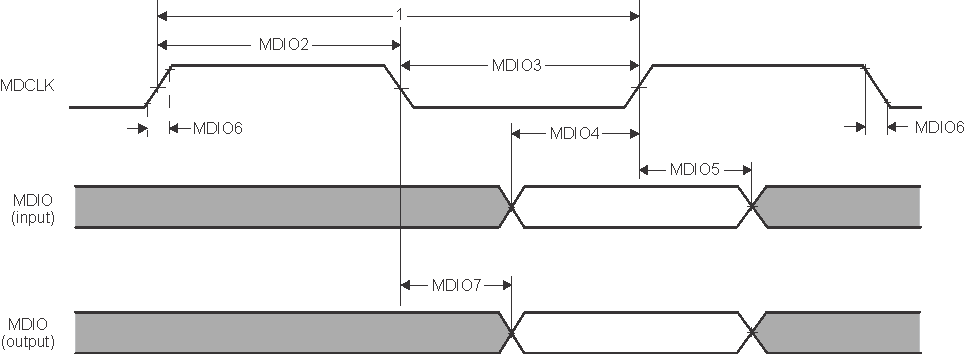
Table 6-7, Table 6-8 and Figure 6-20 present switching characteristics and timing requirements for the MDIO interface.
Table 6-7 Timing Requirements for MDIO Input
| No | PARAMETER | DESCRIPTION | MIN | MAX | UNIT |
|---|---|---|---|---|---|
| MDIO1 | tc(MDC) | Cycle time, MDC | 400 | ns | |
| MDIO2 | tw(MDCH) | Pulse Duration, MDC High | 160 | ns | |
| MDIO3 | tw(MDCL) | Pulse Duration, MDC Low | 160 | ns | |
| MDIO4 | tsu(MDIO-MDC) | Setup time, MDIO valid before MDC High | 90 | ns | |
| MDIO5 | th(MDIO_MDC) | Hold time, MDIO valid from MDC High | 0 | ns |
Table 6-8 Switching Characteristics Over Recommended Operating Conditions for MDIO Output
| NO | PARAMETER | DESCRIPTION | MIN | MAX | UNIT |
|---|---|---|---|---|---|
| MDIO6 | tt(MDC) | Transition time, MDC | 5 | ns | |
| MDIO7 | td(MDC-MDIO) | Delay time, MDC low to MDIO valid | 10 | (P * 0.5) - 10 | ns |
(1) P = MDIO_CLK period in ns.
 Figure 6-20 MAC MDIO diagrams