JAJSND3 December 2024 LM5125-Q1
ADVANCE INFORMATION
- 1
- 1 特長
- 2 アプリケーション
- 3 概要
- 4 Pin Configuration and Functions
- 5 Specifications
-
6 Detailed Description
- 6.1 Overview
- 6.2 Functional Block Diagram
- 6.3
Feature Description
- 6.3.1 Device Configuration (CFG0-pin, CFG1-pin, CFG2-pin)
- 6.3.2 Switching Frequency and Synchronization (SYNCIN)
- 6.3.3 Dual Random Spread Spectrum (DRSS)
- 6.3.4 Operation Modes (BYPASS, DEM, FPWM)
- 6.3.5 Dual- and Multi-phase Operation
- 6.3.6 BIAS (BIAS-pin)
- 6.3.7 Soft Start (SS-pin)
- 6.3.8 VOUT Programming (VOUT, ATRK, DTRK)
- 6.3.9 Protections
- 6.3.10 VOUT Overvoltage Protection (OVP)
- 6.3.11 Thermal Shutdown (TSD)
- 6.3.12 Power-Good Indicator (PGOOD-pin)
- 6.3.13 Current Sensing, Peak Current Limit, and Slope Compensation (CSP1, CSP2, CSN1, CSN2)
- 6.3.14 Current Sense Programming (CSP1, CSP2, CSN1, CSN2)
- 6.3.15 Input Current Limit and Monitoring (ILIM, IMON, DLY)
- 6.3.16 Signal Deglitch Overview
- 6.3.17 MOSFET Drivers, Integrated Boot Diode, and Hiccup Mode Fault Protection (LOx, HOx, HBx-pin)
- 6.4 Device Functional Modes
-
7 Application and Implementation
- 7.1 Application Information
- 7.2
Typical Application
- 7.2.1 Application
- 7.2.2 Design Requirements
- 7.2.3
Detailed Design Procedure
- 7.2.3.1 Determine the Total Phase Number
- 7.2.3.2 Determining the Duty Cycle
- 7.2.3.3 Timing Resistor RT
- 7.2.3.4 Inductor Selection Lm
- 7.2.3.5 Current Sense Resistor Rcs
- 7.2.3.6 Current Sense Filter RCSFP, RCSFN, CCS
- 7.2.3.7 Low-Side Power Switch QL
- 7.2.3.8 High-Side Power Switch QH and Additional Parallel Schottky Diode
- 7.2.3.9 Snubber Components
- 7.2.3.10 Vout Programming
- 7.2.3.11 Input Current Limit (ILIM/IMON)
- 7.2.3.12 UVLO Divider
- 7.2.3.13 Soft Start
- 7.2.3.14 CFG Settings
- 7.2.3.15 Output Capacitor Cout
- 7.2.3.16 Input Capacitor Cin
- 7.2.3.17 Bootstrap Capacitor
- 7.2.3.18 VCC Capacitor CVCC
- 7.2.3.19 BIAS Capacitor
- 7.2.3.20 VOUT Capacitor
- 7.2.3.21 Loop Compensation
- 7.2.4 Application Curves
- 7.3 Power Supply Recommendations
- 7.4 Layout
- 8 Device and Documentation Support
- 9 Revision History
- 10Mechanical, Packaging, and Orderable Information
6.3.17 MOSFET Drivers, Integrated Boot Diode, and Hiccup Mode Fault Protection (LOx, HOx, HBx-pin)
The device integrates N-channel logic MOSFET drivers. The LOx driver is powered by VCC and the HOx driver is powered by HBx. When the SWx-pin voltage is approximately 0V by turning on the low-side MOSFET, the capacitor CHBx is charged from VCC through the internal boot diode. The recommended value of CHBx is 0.1μF. During shutdown, the gate drivers outputs are high impedance.
The LOx and HOx outputs are controlled with an adaptive dead-time methodology, which makes sure that both outputs are not turned on at the same time to prevent shoot through. When the device turns on LOx the adaptive dead-time logic turns off HOx and waits for the HOx-SWx voltage to drop below typically 1.5V, then LOx is turned on after a small dead-time delay tDHL. Also the HOx driver turn-on is delayed until the LOx-PGND voltage has discharged below typically 1.5V. HOx is then turned on after a small dead-time delay tDLH.
If the driver output voltage is lower than the MOSFET gate plateau voltage during start-up, the converter can not start up properly and can be stuck at the maximum duty cycle in a high-power dissipation state. This condition can be avoided by selecting a lower threshold MOSFET or by turning on the device when the BIAS-pin voltage is sufficient. During bypass operation the minimum HOx-SWx voltage is 3.75V.
The hiccup mode fault protection is triggered by HBx-UVLO. If the HBx-SWx voltage is less than the HBx UVLO threshold (VHB-UVLO), LOx turns on by force for 75ns to replenish the boost capacitor. The device allows up to four consecutive replenish switching. After the maximum four consecutive boot replenish switching, the device skips switching for 12 cycles. If the device fails to replenish the boost capacitor after the four sets of the four consecutive replenish switching, the device stops switching and enters 512 cycles of hiccup mode off-time. During the hiccup mode off-time PGOOD = low and the SS-pin is grounded.
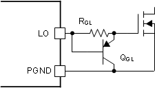
If required the slew rate of the switching node voltage can be adjusted by adding a gate resistor in parallel with pulldown PNP transistor. The resistor can decrease the effective dead-time.
 Figure 6-21 Slew Rate Control