JAJSNK9A December   2021  – December 2022 OPT4001

PRODUCTION DATA  

  1. 特長
  2. アプリケーション
  3. 概要
  4. Revision History
  5. 概要 (続き)
  6. Pin Configuration and Functions
  7. Specifications
    1. 7.1 Absolute Maximum Ratings
    2. 7.2 ESD Ratings
    3. 7.3 Recommended Operating Conditions
    4. 7.4 Thermal Information
    5. 7.5 Electrical Characteristics
    6. 7.6 Typical Characteristics
  8. Detailed Description
    1. 8.1 Overview
    2. 8.2 Functional Block Diagram
    3. 8.3 Feature Description
      1. 8.3.1 Spectral Matching to Human Eye
      2. 8.3.2 Automatic Full-Scale Range Setting
      3. 8.3.3 Output Register CRC and Counter
        1. 8.3.3.1 Output Sample Counter
        2. 8.3.3.2 Output CRC
      4. 8.3.4 Output Register FIFO
      5. 8.3.5 Threshold Detection
    4. 8.4 Device Functional Modes
      1. 8.4.1 Modes of Operation
      2. 8.4.2 Interrupt Modes of Operation
      3. 8.4.3 Light Range Selection
      4. 8.4.4 Selecting Conversion Time
      5. 8.4.5 Light Measurement in Lux
      6. 8.4.6 Light Resolution
    5. 8.5 Programming
      1. 8.5.1 I2C Bus Overview
        1. 8.5.1.1 Serial Bus Address
        2. 8.5.1.2 Serial Interface
      2. 8.5.2 Writing and Reading
        1. 8.5.2.1 High-Speed I2C Mode
        2. 8.5.2.2 Burst Read Mode
        3. 8.5.2.3 General-Call Reset Command
        4. 8.5.2.4 SMBus Alert Response
    6. 8.6 Register Maps
      1. 8.6.1 ALL Register Map
  9. Application and Implementation
    1. 9.1 Application Information
    2. 9.2 Typical Application
      1. 9.2.1 Electrical Interface
        1. 9.2.1.1 Design Requirements
          1. 9.2.1.1.1 Optical Interface
        2. 9.2.1.2 Detailed Design Procedure
          1. 9.2.1.2.1 Optomechanical Design (PicoStar Variant)
          2. 9.2.1.2.2 Optomechanical Design (SOT-5X3 Variant)
        3. 9.2.1.3 Application Curves (PicoStar Variant)
    3. 9.3 Do's and Don'ts
    4. 9.4 Power Supply Recommendations
    5. 9.5 Layout
      1. 9.5.1 Layout Guidelines
      2. 9.5.2 Layout Example
        1. 9.5.2.1 Soldering and Handling Recommendations (SOT-5X3 Variant)
        2. 9.5.2.2 Soldering and Handling Recommendations (PicoStar Variant)
          1. 9.5.2.2.1 Solder Paste
          2. 9.5.2.2.2 Package Placement
          3. 9.5.2.2.3 Reflow Profile
          4. 9.5.2.2.4 Special Flexible Printed-Circuit Board (FPCB) Recommendations
          5. 9.5.2.2.5 Rework Process
  10. 10Device and Documentation Support
    1. 10.1 Documentation Support
      1. 10.1.1 Related Documentation
    2. 10.2 ドキュメントの更新通知を受け取る方法
    3. 10.3 サポート・リソース
    4. 10.4 Trademarks
    5. 10.5 静電気放電に関する注意事項
    6. 10.6 用語集
  11. 11Mechanical, Packaging, and Orderable Information

Soldering and Handling Recommendations (SOT-5X3 Variant)

The OPT4001 has been qualified for three soldering reflow operations per JEDEC JSTD-020.

Note that excessive heat can discolor the device and affect optical performance.

See application report SLUA271, QFN/SON PCB Attachment, for details on soldering thermal profile and other information. If the OPT4001 must be removed from a PCB, discard the device and do not reattach.

As with most optical devices, handle the device with special care to make sure that optical surfaces stay clean and free from damage. See Section 9.3 for more detailed recommendations. For best optical performance, solder flux and any other possible debris must be cleaned after soldering processes.
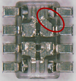
GUID-20221114-SS0I-HPJV-C8QM-1LFMTJ1ZQWXV-low.png
Note: The bottom side of the device features an angled feature to denote the PIN 1
Figure 9-14 Identification Feature for PIN 1
GUID-20221114-SS0I-PGXH-KQGH-LBF50V23NLS3-low.png Figure 9-15 Identification Features for PIN 1 on Package