JAJSOE3B August 2022 – September 2024 ULN2803C
PRODUCTION DATA
- 1
- 1 特長
- 2 アプリケーション
- 3 概要
- 4 Pin Configuration and Functions
- 5 Specifications
- 6 Parameter Measurement Information
- 7 Detailed Description
- 8 Application and Implementation
- 9 Device and Documentation Support
- 10Revision History
- 11Mechanical, Packaging, and Orderable Information
4 Pin Configuration and Functions
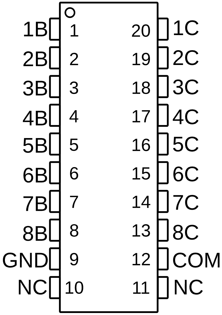
 Figure 4-1 DW Package,20-Pin SOIC(Top View)
Table 4-1 Pin Functions
| PIN | TYPE | DESCRIPTION | |
|---|---|---|---|
| NAME | NO. | ||
| 1B | 1 | I | Channel 1 through 8 Darlington base input. |
| 2B | 2 | ||
| 3B | 3 | ||
| 4B | 4 | ||
| 5B | 5 | ||
| 6B | 6 | ||
| 7B | 7 | ||
| 8B | 8 | ||
| 1C | 20 | O | Channel 1 through 8 Darlington collector output. |
| 2C | 19 | ||
| 3C | 18 | ||
| 4C | 17 | ||
| 5C | 16 | ||
| 6C | 15 | ||
| 7C | 14 | ||
| 8C | 13 | ||
| GND | 9 | — | Common emitter shared by all channels (typically tied to ground). |
| COM | 12 | I/O | Common cathode node for flyback diodes (required for inductive loads). |
|
NC |
10, 11 |
— | No connect pin. |