JAJSOR8 September 2024 LM70840 , LM70860 , LM70880
PRODUCTION DATA
- 1
- 1 特長
- 2 アプリケーション
- 3 概要
- 4 Pin Configuration and Functions
- 5 Specifications
-
6 Detailed Description
- 6.1 Overview
- 6.2 Functional Block Diagram
- 6.3
Feature Description
- 6.3.1 Input Voltage Range (VIN)
- 6.3.2 High-Voltage Bias Supply Regulator (VCC, BIAS, VDDA)
- 6.3.3 Enable (EN)
- 6.3.4 Power-Good Monitor (PG)
- 6.3.5 Switching Frequency (RT)
- 6.3.6 Dual Random Spread Spectrum (DRSS)
- 6.3.7 Soft Start
- 6.3.8 Output Voltage Setpoint (FB)
- 6.3.9 Minimum Controllable On-Time
- 6.3.10 Error Amplifier and PWM Comparator (FB, EXTCOMP)
- 6.3.11 Slope Compensation
- 6.3.12 Shunt Current Sensing
- 6.3.13 Hiccup Mode Current Limiting
- 6.3.14 Device Configuration (CONFIG)
- 6.3.15 Single-Output Dual-Phase Operation
- 6.3.16 Pulse Frequency Modulation (PFM) / Synchronization
- 6.3.17 Thermal Shutdown (TSD)
- 6.4 Device Functional Modes
-
7 Application and Implementation
- 7.1 Application Information
- 7.2
Typical Applications
- 7.2.1
Design 1 – High Efficiency, Wide Input, 400kHz Synchronous Buck
Regulator
- 7.2.1.1 Design Requirements
- 7.2.1.2
Detailed Design Procedure
- 7.2.1.2.1 Custom Design With WEBENCH® Tools
- 7.2.1.2.2 Custom Design With Excel Quickstart Tool
- 7.2.1.2.3 Buck Inductor
- 7.2.1.2.4 Current-Sense Resistance
- 7.2.1.2.5 Output Capacitors
- 7.2.1.2.6 Input Capacitors
- 7.2.1.2.7 Frequency Set Resistor
- 7.2.1.2.8 Feedback Resistors
- 7.2.1.2.9 Compensation Components
- 7.2.1.3 Application Curves
- 7.2.2 Design 2 – High Efficiency 48V to 12V 400kHz Synchronous Buck Regulator
- 7.2.1
Design 1 – High Efficiency, Wide Input, 400kHz Synchronous Buck
Regulator
- 7.3 Power Supply Recommendations
- 7.4 Layout
- 8 Device and Documentation Support
- 9 Revision History
- 10Mechanical, Packaging, and Orderable Information
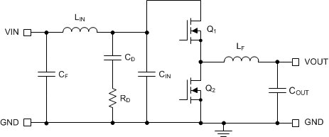
7.1.1.4 EMI Filter
Switching regulators exhibit negative input impedance, which is lowest at the minimum input voltage. An underdamped LC filter exhibits a high output impedance at the resonant frequency of the filter. For stability, the filter output impedance must be less than the absolute value of the converter input impedance.
The EMI filter design steps are as follows:
- Calculate the required attenuation of the EMI filter at the switching frequency, where CIN represents the existing capacitance at the input of the switching converter.
- Input filter inductor LIN is usually selected between 1μH and 10μH, but can be lower to reduce losses in a high-current design.
- Calculate input filter capacitor CF.
 Figure 7-2 Buck Regulator With π-Stage EMI Filter
By calculating the first harmonic current from the fourier series of the input current waveform and multiplying the result by the input impedance (the impedance is defined by the existing input capacitor CIN), a formula is derived to obtain the required attenuation as shown by Equation 18.
where
- VMAX is the allowed dBμV noise level for the applicable conducted EMI specification, for example CISPR 25 Class 5.
- CIN is the existing input capacitance of the buck regulator.
- DMAX is the maximum duty cycle.
- IPEAK is the peak inductor current.
For filter design purposes, the current at the input can be modeled as a square-wave. Determine the EMI filter capacitance CF from Equation 19.
Adding an input filter to a switching regulator modifies the control-to-output transfer function. The output impedance of the filter must be sufficiently small such that the input filter does not significantly affect the loop gain of the buck converter. The impedance peaks at the filter resonant frequency. The resonant frequency of the filter is given by Equation 20.
The purpose of RD is to reduce the peak output impedance of the filter at the resonant frequency. Capacitor CD blocks the DC component of the input voltage to avoid excessive power dissipation in RD. Capacitor CD must have lower impedance than RD at the resonant frequency with a capacitance value greater than that of the input capacitor CIN. This prevents CIN from interfering with the cutoff frequency of the main filter. Added damping is needed when the output impedance of the filter is high at the resonant frequency (Q of filter formed by LIN and CIN is too high). An electrolytic capacitor CD can be used for damping with a value given by Equation 21.
Select the damping resistor RD using Equation 22.