JAJSP62G December 2002 – September 2022 SN65HVD20 , SN65HVD21 , SN65HVD22 , SN65HVD23 , SN65HVD24
PRODUCTION DATA
- 1 特長
- 2 アプリケーション
- 3 概要
- 4 Revision History
- 5 概要 (続き)
- 6 Device Comparison
- 7 Pin Configuration and Functions
-
8 Specifications
- 8.1 Absolute Maximum Ratings
- 8.2 ESD Ratings
- 8.3 Recommended Operating Conditions
- 8.4 Thermal Information
- 8.5 Driver Electrical Characteristics
- 8.6 Receiver Electrical Characteristics
- 8.7 Driver Switching Characteristics
- 8.8 Receiver Switching Characteristics
- 8.9 Receiver Equalization Characteristics
- 8.10 Power Dissipation
- 8.11 Typical Characteristics
- 9 Parameter Measurement Information
- 10Detailed Description
- 11Application and Implementation
- 12Power Supply Recommendations
- 13Layout
- 14Device and Documentation Support
- 15Mechanical, Packaging, and Orderable Information
9 Parameter Measurement Information
Note:
Test load capacitance includes probe and jig capacitance (unless otherwise specified). Signal generator characteristics: rise and fall time < 6 ns, pulse rate 100 kHz, 50% duty cycle, ZO = 50 Ω (unless otherwise specified).
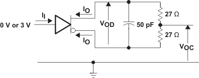 Figure 9-1 Driver Test Circuit, VOD and VOC Without Common-Mode Loading
 Figure 9-2 Driver Test Circuit, VOD With Common-Mode Loading
 Figure 9-3 Driver Switching Test Circuit and Waveforms
 Figure 9-4 Driver VOC Test Circuit and Waveforms
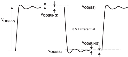
VOD(RING) is measured at four points on the output waveform, corresponding to overshoot and undershoot from the VOD(H) and VOD(L) steady state values.
Figure 9-5 VOD(RING) Waveform and Definitions Figure 9-6 Driver Enable and Disable Test, High Output
 Figure 9-7 Driver Enable and Disable Test, Low Output
 Figure 9-8 Driver Standby and Wake Test Circuit and Waveforms
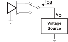 Figure 9-9 Driver Short-Circuit Test
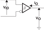 Figure 9-10 Receiver DC Parameter Definitions
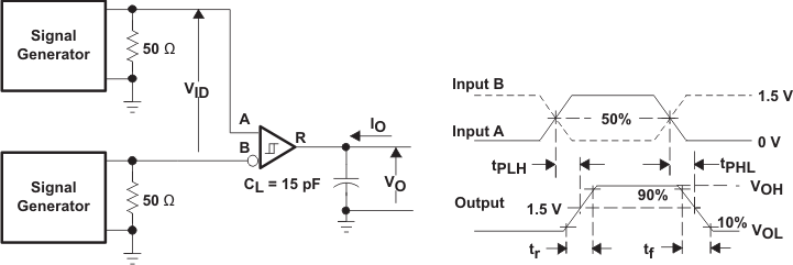 Figure 9-11 Receiver Switching Test Circuit and Waveforms
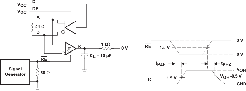 Figure 9-12 Receiver Enable Test Circuit and Waveforms, Data Output High
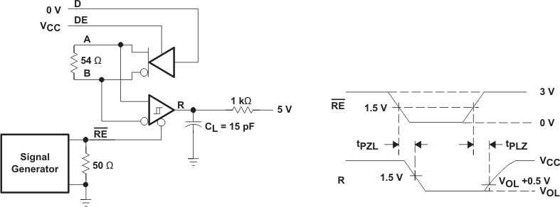 Figure 9-13 Receiver Enable Test Circuit and Waveforms, Data Output Low
 Figure 9-14 Receiver Standby and Wake Test Circuit and Waveforms
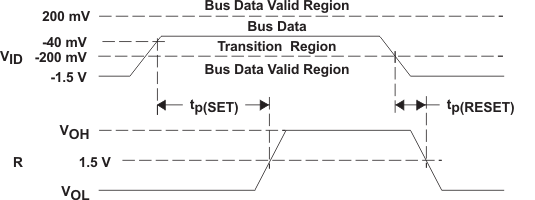 Figure 9-15 Receiver Active Failsafe Definitions and Waveforms
 Figure 9-16 Test Circuit and Waveforms, Transient Overvoltage Test